Everything related to digital electronics is related to time. Timer, counter, frequency, pulse width, clock and time are the most common words one may find in this arena. Microcontrollers just like humans need heart-beats and these come from clock sources. Apart from system clock, timers are clock sources that can be used as heart-beats for various applications. All modern micros are embedded with timer-counter modules and generally they are used for generating time bases, counting pulses, measuring time periods of waveforms, generating pulse width modulation (PWM) signals, triggering external devices and timing special events. STM32 micros have several timers designed for such applications. However unlike most 8-bit micros which possess two/three timers with limited functionalities, the timers of STM32s are very elaborate and complex. This explains why documentations related to timer modules take about 25% of any STM32 reference manual.
 Before we begin exploring STM32 timers, I must point out that I won’t be able to cover every aspect of all timer modules as they are vast and need lot of explanations, something which is beyond the scope of a single post. This is why in this issue we shall explore the very basics of timer modules enough to get STM32 timers to work.
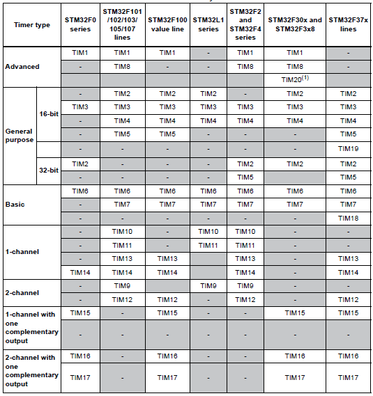
Classification of STM32 Timers
The timers in a STM32 micro can be classified as follows:
- Advanced Timers
- General Purpose Timers
- Basic Timers
Of these three types of timers the first two are common to all. The third is available only in larger variants. The number of timers of a given class also varies with the capacity or the size of the STM32 micro. For instance, STM32F103C8T6 has one advance timer while STM32F103VET6 has two advanced timers. STM32CubeMX can be used to determine which timers are available in a given STM32 micro unless you wish to get lost in piles of documentations.

In my own words, I will describe STM32 timer as follows.
General purpose (GP) timers have all the features of a typical timer-counter module. They are pretty much the same as the ones we have seen in most 8-bit micros. They can be used for any timer-counter-related purpose and so they are named as such. PWM generation, input capture, time-base generation and output compare are the basic uses of a GP timer. Typically in a STM32 micro you’ll find more GP timers than other classes of timers. Studying GP timers clears the basic concepts.
Basic timers are timers that don’t have I/O channels for input capture/PWM generation and so they are strictly used for time-base generation purposes. Basic timers are available only in large capacity STM32 micros and are the simplest of all timers.
Advanced timers are almost the same as GP timers but they additionally have the ability to generate complementary PWM signals as well as generate brake and dead-time for such signals. These features make them suitable for applications related to motor control, inverters, SMPSs and other power electronics-related tasks. In most STM32 micros, there is at least one such timer. In larger STM32s, there can be two.
Every timer in a STM32 micro is independent of the others and so they don’t share any common resource. The only things that are common are the register types, naming convention and their operating principles. With only a few exceptions, timer modules are more-or-less compatible amongst STM32 micro families. You’ll not find significant differences when you migrate from STM32F1xx series to STM32F4xx series. This is not true for other internal hardware like GPIO ports, ADCs, etc.
Timer Overview
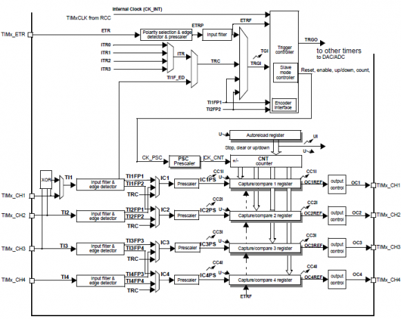
Typically most STM32 timers consist of a 16-bit auto reload counter and a 16-bit prescaler. The prescaler is responsible for dividing the incoming clock signal from a clock source as per our need. The auto-reload counter is loaded just we used to load timer registers of 8-bit MCUs. The only thing exceptional about it is its auto reloading feature. In old school 8-bit MCUs, we needed to reload the timer after every interrupt or after every overflow. This is not required in STM32s as it is automatically handled.
Unlike most other MCUs in which timers usually count incrementally, STM32 timers can count up, down or center-aligned. However in most applications up counting is more preferable over other methods.
With the exception of basic timers, all STM32 timers have four independent I/O channels (TIMx_CH1 – TIMx_CH4). These can be used as follows:
- Input Capture
- Output Compare or PWM
- One Pulse Mode
Timers can be clocked by:
- Internal Clock
- External Clock Sources
- External Mode 1 (TI1 and TI2 pins)
- External Mode 2 (ETR pin)
- Internal Trigger (ITRx)
Interrupt and DMA events occur when the followings occur:
- Update
- Counter overflow/underflow
- Counter initialized
- Others
- Trigger
- Counter Start
- Counter Stop
- Counter Initialize
- Others
- Input Capture / Output Compare
- Others
The table below summarizes some common features of STM32 timers.
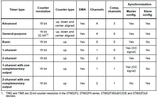
From all of these info we can draw the versatility of STM32 timers although they are not very easy to deal with in the beginning. This is why unlike my previous tutorials on other STM32 peripherals, we will study the timers concurrently with their applications and coding.
Timer Registers
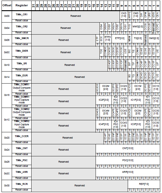
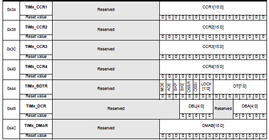
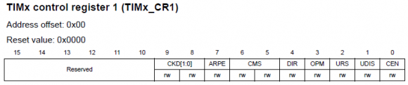
Before we start coding, I must point out that perhaps the most complex sets of registers in a STM32 micro belong to timer-counter modules. We don’t need all of them for a specific application and so to avoid complexity we will only discuss about those registers that we will be needing for a particular task. A few registers will always be needed but other will needed for specific tasks like input capture/ output compare. Another important thing to note on these registers is the fact that though all registers in an ARM micro are 32-bit wide, for timer modules and most hardware peripherals most of the bits are reserved. This makes handling them easy. To yet simplify handling these during coding I have used my own built definitions and functions similar to ST’s SPL. MikroC libraries also take care some of such. Just for reference check out the register map of any timer module. I have shown one below.
Design Considerations
A few things should be remembered before coding and designing hardware. These are as follows:
- Timer modules to be used should be enabled first by setting appropriate RCC_APBx_ENR register bits. Individual counters, DMA and interrupts are enabled after setting up everything else.
- Right after power on reset every bit of internal registers of a STM32 micro are in their default reset values. For timer registers the default is all zeroes, meaning everything disabled. Thus the ones we don’t need to use, need not to be forcefully cleared. Usually this is the case for most internal hardware peripherals. However if you need to change stuffs on the fly, you better reset all settings just to avoid running down to the jaws of a software bug or unprecedented results.
- Timers can’t be used like RTCs for a number of factors and so it is not always wise to use them as precision time keepers. If accuracy is not very important, timers can be used for general time-keeping purposes. No doubt timers are accurate than wasteful delay functions but they are not good as dedicated RTCs.
- When using GPIOs for capture/compare mode, make sure which I/O pins are being used because sometimes the I/O pins related to these functionalities can be remapped elsewhere. Use STM32CubeMX to find out which pins can be used with a given timer.
- AFIO block must be enabled and used for remapping I/O pins since capture/compare are alternative functions of ordinary GPIOs. AFIO block should be enabled even if remapping is not used. GPIOs should be configured as AFIOs for compare/output modes.
- When using input capture mode, be sure of the maximum input voltage level of an incoming waveform. Not all but most I/O pins are 5V tolerant. I will however strongly suggest not to cross the VDD limit, typically 3.3V. Similarly when using compare mode, be sure that the end device like a LED or an opto-coupler connected to a compare pin doesn’t draw too much current. Simply do not exceed the specified GPIO electrical specs. This is very important.
- The internal oscillator of STM32 micros are quite accurate (1% tolerant) but if more precision is needed, it is better to use well calibrated external clock generators or precise external crystals.
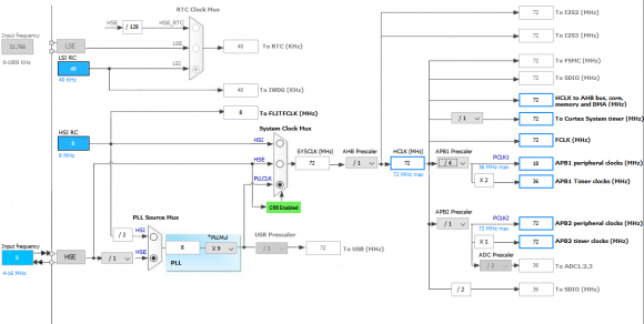
- Be aware of clock system prescalers, multipliers and clock sources.
- Remember APB2 bus peripherals can run at maximum system clock speed while APB1 bus peripherals are limited to half of that speed. Thus APB1 timers may not run at the same clock speed as the APB2 timers.
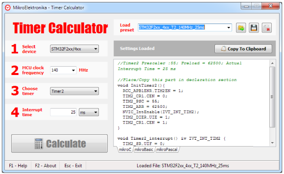
- Since internal clock speed of each timer is dependent on its APB bus speed, it is a must know to which APB bus a given timer belongs. On MikroE’s Timer Calculator utility software this is actually the MCU clock speed. Use STM32CubeMX and MikroC compiler’s project editor to determine APB bus speeds. I have shown an example below. Here APB1 timers are being fed with 36MHz while APB2 timers are being fed by 72MHz.
Hardware and Software
As with the previous issues, MikroC for ARM C compiler is what we will be using. Except the code examples which are dependent on MikroC compiler’s library functions, most of the codes can be ported to other compilers. We’ll also get introduced with a new software tool and obviously STM32CubeMx and ST-Link software will play their parts. I’ll also use my developed SPL libraries.
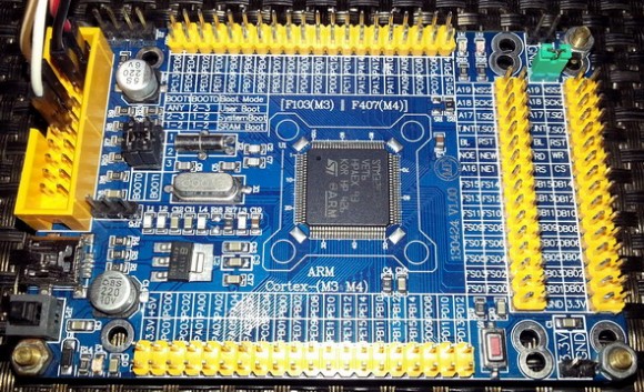
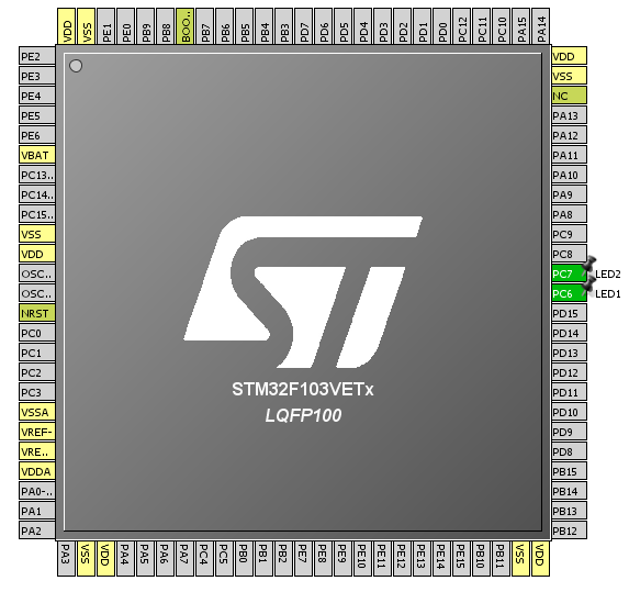
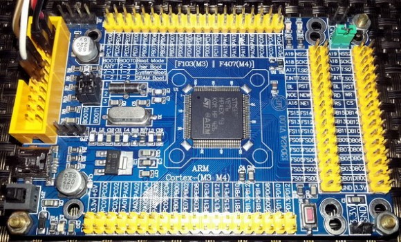
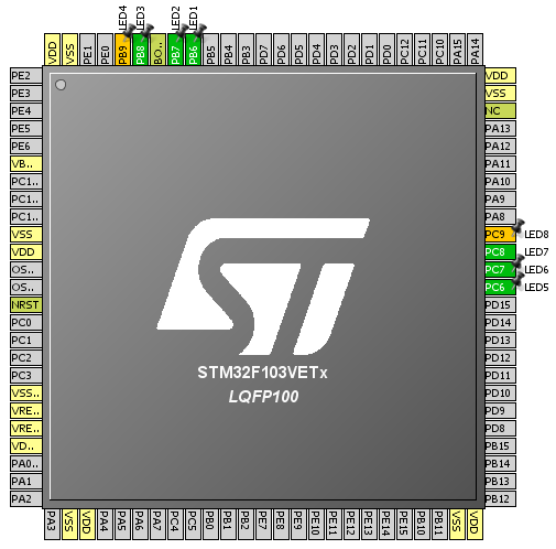
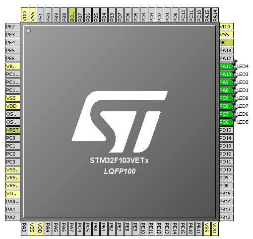
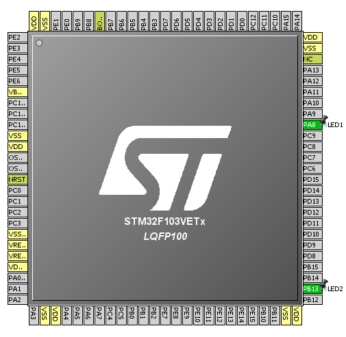
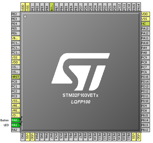
The hardware that I’ll introduce here is a STM32F103VET6 ARM Cortex M3 development board. I chose this micro as it has all types of timer I discussed, eight timers – two advance timers, two basic timers and four GP timers. In terms of all hardware resources, it is a beast that comes in a LQFP100 SMD package with 512kB of flash, 64kB of RAM and 82 I/Os. The board on which it is embedded is also neatly designed with proper readable labels – simply a nice STM32 development board.
Time Base Generation
This is most basic use of a timer. In this mode of operation, we will have to program the timer as such that it’ll periodically generate timed events. For this purpose we can use any timer but I recommend using either GP timers or basic timer (if any). There is no specific reason for this recommendation. It is just my way of using STM32 timers – use things that have been designed for their purposes.
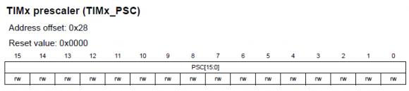
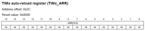
For making time base generators we need to follow a few steps and the overall thing is very easy. We will use interrupt-based method. First we need to determine which timer we will be using and what should be the frequency of the timer interrupt. We, then, need to calculate the values for the prescaler (PSC), the auto-reload register (ARR) and the repetition counter (RCR) (if any). Repetition counters are available only in advanced timers only. We can use the following formula for determining interrupt rate:
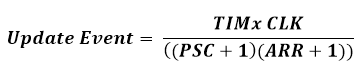 RCR will be zero unless used or available and so generally the formula will be:
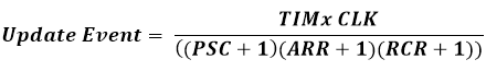 TIMx clock is dependent on APB bus clock.
Finally we will be enabling timer interrupts and the counter module itself.
Sometime along its path in the world of embedded systems, MikroElektronika (MikroE), a well-reputed microcontroller-based hardware and software solution provider, developed a free tool called Timer Calculator. This tool made life easy. We can use it to generate codes necessary for timer interrupts. It generate codes for MikroC, MikroBasic or MikroPascal. Originally Timer Calculator used support PIC and AVR platforms only but recently after unveiling MikroE ARM compilers, ARM platforms were incorporated with it. If we have fairly some sound idea of how things are working inside a STM32, we can avoid all the time-consuming, tiring silly calculations and use it to complete your job easily. We just need to select the STM32 family, MCU clock and desired interrupt rate either in terms of time or in terms of frequency. There are also some preset code examples than can also be used to get a head start.
Timer Calculator can be downloaded from here:
http://www.libstock.com/projects/view/398/timer-calculator.
In terms of registers we just need to deal with the following registers only when we need to generate time-bases. I will not explain them in details as their coding will do that.
Code Examples
MikroE Timer Calculator Example
There’s nothing to say about this example as the software says for itself. We just need to the stuffs as marked in the image below. In this example two LEDs connected to GPIOC pin 6 and 7 will toggle logic states every 500ms. Pin C7 LED flashes due to timer 6 update interrupt and pin C6 LED blinks due one main loop execution. After every interrupt, interrupt flags in the timer status registers need to be cleared.
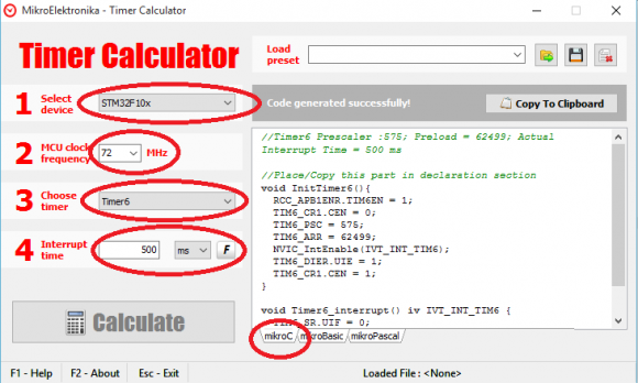
The following setup is used for this code example and the next.
void setup();
void GPIO_init();
void Timer6_init();
void TIM6_ISR()
iv IVT_INT_TIM6
ics ICS_AUTO
{
TIM6_SR.UIF = 0;
GPIOC_ODRbits.ODR7 ^= 1;
}
void main()
{
setup();
while(1)
{
GPIOC_ODRbits.ODR6 ^= 1;
delay_ms(500);
};
}
void setup()
{
GPIO_init();
Timer6_init();
}
void GPIO_init()
{
GPIO_Clk_Enable(&GPIOC_BASE);
GPIO_Config(&GPIOC_BASE,
(_GPIO_PINMASK_6 | _GPIO_PINMASK_7),
(_GPIO_CFG_MODE_OUTPUT | _GPIO_CFG_SPEED_MAX | _GPIO_CFG_OTYPE_PP));
GPIOC_ODRbits.ODR6 = 0;
GPIOC_ODRbits.ODR7 = 0;
}
void Timer6_init()
{
RCC_APB1ENR.TIM6EN = 1;
TIM6_CR1.CEN = 0;
TIM6_PSC = 575;
TIM6_ARR = 62499;
NVIC_IntEnable(IVT_INT_TIM6);
EnableInterrupts();
TIM6_DIER.UIE = 1;
TIM6_CR1.CEN = 1;
}
Demo video link: https://www.youtube.com/watch?v=L3TVU7BGK9s.
There are some ignorable limitations of the MikroE Timer Calculator software. For instance it doesn’t support advance timers but I don’t find it as a problem. You can use any other timer like Timer 4 for instance, generated codes for it and then renumber/rename the registers. Another reason for which I’m not bothered by this is due to the fact that advance timers are meant for dedicated advanced tasks and not for silly time-keeping.
Multiple Timer Interrupt Example
This example is just like the previous one except this time the code is written with my SPL functions and two timers are running simultaneously with different clock frequencies. LEDs connected to GPIOC 6 and 7 pins flash to show the update rates of these timers. An advance and a GP timer are used in the demo.
#include "TIM_common.h"
#include "TIM3.h"
#include "TIM8.h"
#include "GPIO.h"
void setup();
void GPIO_init();
void Timer3_init();
void Timer8_init();
void TIM3_ISR()
iv IVT_INT_TIM3
ics ICS_AUTO
{
TIM3_SR = 0;
GPIOC_pin_toggle(6);
}
void TIM8_ISR()
iv IVT_INT_TIM8_UP
ics ICS_AUTO
{
TIM8_SR = 0;
GPIOC_pin_toggle(7);
}
void main()
{
setup();
while(1)
{
};
}
void setup()
{
GPIO_init();
Timer3_init();
Timer8_init();
}
void GPIO_init()
{
enable_GPIOC(true);
setup_GPIOC(6, (GPIO_PP_output | output_mode_medium_speed));
setup_GPIOC(7, (GPIO_PP_output | output_mode_medium_speed));
}
void Timer3_init()
{
enable_TIM3(true);
enable_TIM3_counter(false);
TIM3_PSC = 575;
TIM3_ARR = 62499;
set_TIM3_counting_direction(down_counting);
NVIC_IntEnable(IVT_INT_TIM3);
EnableInterrupts();
enable_TIM3_update_interrupt(true);
enable_TIM3_counter(true);
}
void Timer8_init()
{
enable_TIM8(true);
enable_TIM8_counter(false);
TIM8_PSC = 575;
TIM8_ARR = 62499;
set_TIM8_counting_direction(up_counting);
NVIC_IntEnable(IVT_INT_TIM8_UP);
EnableInterrupts();
enable_TIM8_update_interrupt(true);
enable_TIM8_counter(true);
}
Demo video link: https://www.youtube.com/watch?v=jyPUu5JqZyU.
External Clock Drive/Counter Example
In the beginning I stated that timers can be driven with external clock sources. STM32 timers can be driven with three types of external sources. We can use this facility to count pulses coming from a sensor like a Hall position sensor. We can also cascade several such timers to form a high precision timer. In this example, we will see how this is done.
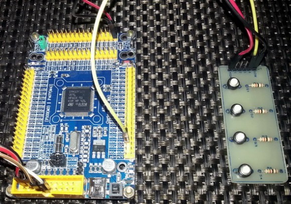
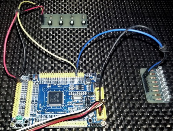
The following hardware setup is used.
Please refer to the code. Note GPIOA 0 pin is used as the input of the external clock source. Here I connected a button to stimulate the external clock source. Note that the AFIO block has been enabled but no pin remapping is used. I avoided pin remapping to keep things simple although pin remapping is not hard. The following code sets up external clock properties.
set_TIM2_clock_division(clock_division_tCK_INT);
set_TIM2_CC1_selection(CC1_input_IC1_on_TI1);
set_TIM2_CC1_state_and_polarity(enable, rising_edge);
set_TIM2_trigger_source(TI1_edge_detector);
set_TIM2_slave_selection(external_clock_mode_1);
As you can see the external clock source will only be sensed during rising edge transitions. Its input channel enabled and selected.
The rest of the code in the timer setup simply state how much to count before invoking an interrupt and should there be any prescaling for the incoming signal. This code makes my STM32 board sense two rising edges before invoking an interrupt and toggling a LED connected to GPIOC 6 pin. Pretty simple.
#include "TIM_common.h"
#include "TIM2.h"
#include "AFIO.h"
#include "GPIO.h"
void setup();
void setup_IO();
void setup_TIM2();
void TIM2_ISR()
iv IVT_INT_TIM2
ics ICS_AUTO
{
TIM2_SR = 0;
GPIOC_pin_toggle(6);
}
void main()
{
setup();
while(1);
}
void setup()
{
setup_IO();
setup_TIM2();
}
void setup_IO()
{
AFIO_enable(true);
AFIO_remap(TIM2_not_remapped);
enable_GPIOA(true);
setup_GPIOA(0, input_without_pull_resistors);
enable_GPIOC(true);
setup_GPIOC(6, (GPIO_PP_output | output_mode_high_speed));
GPIOC_pin_high(6);
}
void setup_TIM2()
{
enable_TIM2(true);
enable_TIM2_counter(false);
TIM2_ARR = 0x0002;
TIM2_PSC = 0x0000;
set_TIM2_counting_direction(up_counting);
set_TIM2_clock_division(clock_division_tCK_INT);
set_TIM2_CC1_selection(CC1_input_IC1_on_TI1);
set_TIM2_CC1_state_and_polarity(enable, rising_edge);
set_TIM2_trigger_source(TI1_edge_detector);
set_TIM2_slave_selection(external_clock_mode_1);
enable_TIM2_update_interrupt(true);
NVIC_IntEnable(IVT_INT_TIM2);
EnableInterrupts();
enable_TIM2_counter(true);
}
Demo video link: https://www.youtube.com/watch?v=jCVWCoJeqec.
Pulse Width Modulation (PWM)
Pulse Width Modulation (PWM) is another feature that is common in most modern MCUs. With PWM outputs, we can generate waveforms as per our need and so often it is said that PWMs mimic analogue outputs. In reality PWMs don’t output continuous analogue voltages like Digital-Analogue Converters but rather output variable width pulses that have average values. A low-pass RC filter can be used to obtain continuous output voltages while blocking high frequency PWM waveform components.
All STM32s have timer-counter modules. Except basic timers, all STM32 timers are capable of generating PWM outputs. Each timer has four such outputs called PWM channels. Advance timers have up to seven PWM channels each – six for complementary PWM and a single channel. Now you can see that even a small STM32 micro has many PWM channels unlike most other MCUs. What’s more interesting is the fact that these PWM channels are not fixed to some dedicated GPIO port pins, some can be remapped elsewhere.
In any work, there are two ways – the easy way and the hard way. Both ways have their cons and pros. Yeah I’m taking about MikroC’s PWM library. MikroE packed their compilers with libraries literally for everything inside a micro and PWM library is just another example. These libraries are easy to use. With minimum knowledge one can work wonders with such libraries. Prototyping an idea from abstracts then becomes a matter of a few lines of code. However as a developer MikroE can’t provide solution for all possible permutations and combinations. Sometimes even from the point of view of a programmer that’s unnecessary and so they only provide the basic libraries that are mostly used. In such cases it the responsibility of a coder to code stuffs as required. Too much library dependence is also not good for smart coding.
We already dealt with four registers for generating time bases. Apart from those we need a few more registers for PWM generation. Actually three sets of registers are needed to be dealt with. For advance timers, we will need to handle one more register for dead time and other purposes apart from the other three.
Firstly I will introduce the timer capture/compare mode register set. This set comprises of two separate registers TIMx_CCMR1 and TIMx_CCMR2. TIMx_CCMR1 controls capture/compare channel 1 and 2 while channel 3 and 4 are controlled by TIMx_CCMR2.
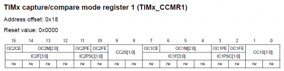
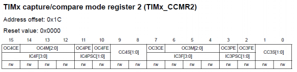
Please note that unlike other registers the CCMR registers have dual role and so the register maps have two separations. The top rows of these registers are for output/compare mode while the bottom layers are for input capture mode. CCxS bits of these registers determine the corresponding capture/compare channel’s I/O direction. For PWM mode these bits will be zero. The next stuff that we need to set in these registers are OCxM bits. These bits should be set either as 110 or 111 for PWM mode. The difference in these two bit settings is the PWM output type – i.e. normal PWM or inverted PWM.
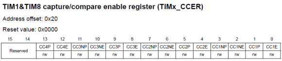
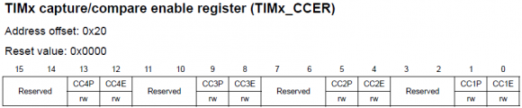
The next set of registers we will be dealing with are the TIMx_CCER registers. For all timers their bit orientations are same but advance timers have additional bits for additional functionalities. The purposes of these registers are simply enabling the desired capture/compare channels and setting their polarities.
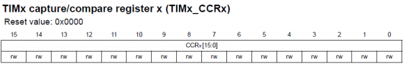
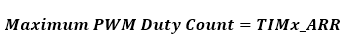
For every timer except the basic ones, there are four capture/compare registers TIMx_CCRx which correspond to four capture/compare channels. Changing the values in them during compare mode allows us to change PWM width or duty cycle. The value that will be set in the TIMx_ARR register will correspond to maximum PWM count or 100% duty cycle. PWM generation is accomplished by comparing the values in TIMx_CCRx registers and TIMx_CNT register. Note that complementary channels have no such registers and that’s because they output complementary signals of their respective ordinary channels.
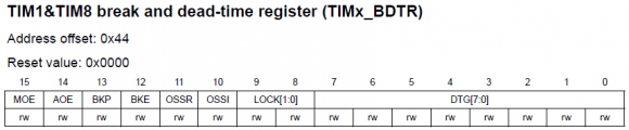
The registers I mentioned so far are common to all timers with capture/compare functionalities. Using them will allow us to accomplish common PWM-related tasks. However there is one more register that we will be needing to handle for more advanced tasks and so it is available only in advanced timers. This register is called Timer Brake and Dead Time Register, TIMx_BDTR. It is important to note that when using advanced timers for PWM generation the MOE bit should be set or else there will be no PWM output.
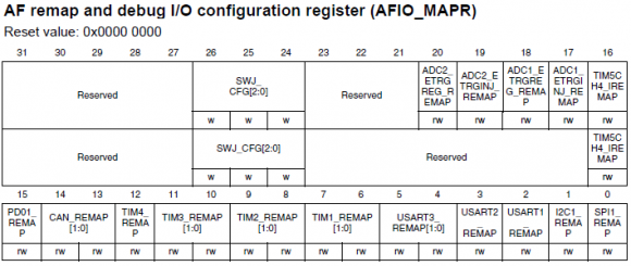
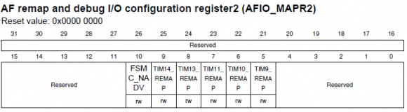
Since PWM generation and input capture are alternative functions of a GPIO pin, we need to enable and use AFIO registers as well for alternative functions of those pins. Provided it is supported, with AFIO registers we can remap/reposition default PWM/input capture pins to some other pins. AFIO_MAPR and AFIO_MAPR2 registers are used for such purposes.
Code Examples
MikroC PWM Library Example
All MikroC compilers come with PWM libraries. MikroC for ARM has PWM libraries for different variants of ARM chips – Stellaris M3s, M4s and STM32s. We are only concerned with STM32 variants. Only four functions are what are needed to be understood for using this library and these are as follows:
- PWM_TIMn_Init – initializes timer module in PWM mode by setting desired PWM frequency.
- PWM_TIMn_Set_Duty – sets PWM duty, PWM type and channel.
- PWM_TIMn_Start – starts respective timer module in PWM mode.
- PWM_TIMn_Stop – stops respective timer module.
As you can see these built-in library functions are very easy to get started with. However be sure of pin remapping. Random pin remapping may lead to undesired problems. Remember pins are mapped in groups. This is the common mistake most people make with PWM library.
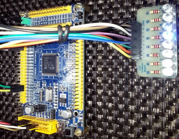
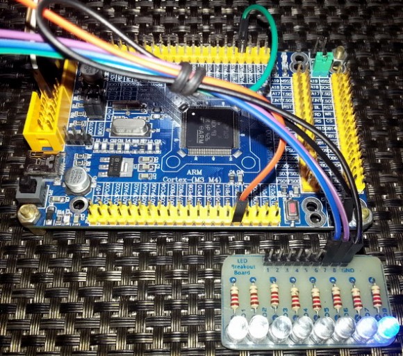
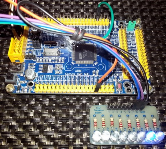
The code example for this demo is a glowing-fading running light. General purpose timers 3 and 4 are used to generate 6 kHz PWMs in eight channels. At any instance two adjacent LEDs will glow and fade opposite to each other. The brightness of one will gradually increase with the gradual decrement of the pervious LED’s brightness.
Note that in the code I didn’t set the AFIO registers and I also didn’t enable the timer APB buses. This is the advantage of using MikroC libraries. The PWM library took care of these.
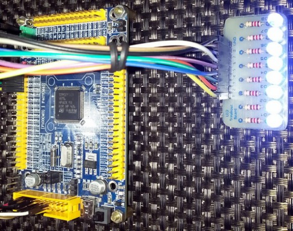
The following hardware setup is used for this demo:
unsigned int pwm_val = 0;
void setup();
void setup_PWMs();
void main()
{
unsigned int i = 0;
setup();
while(1)
{
for(i = 0; i <= pwm_val; i++)
{
PWM_TIM4_Set_Duty(i, _PWM_INVERTED, _PWM_CHANNEL1);
PWM_TIM4_Set_Duty(i, _PWM_NON_INVERTED, _PWM_CHANNEL2);
delay_us(200);
}
for(i = 0; i <= pwm_val; i++)
{
PWM_TIM4_Set_Duty(i, _PWM_INVERTED, _PWM_CHANNEL2);
PWM_TIM4_Set_Duty(i, _PWM_NON_INVERTED, _PWM_CHANNEL3);
delay_us(200);
}
for(i = 0; i <= pwm_val; i++)
{
PWM_TIM4_Set_Duty(i, _PWM_INVERTED, _PWM_CHANNEL3);
PWM_TIM4_Set_Duty(i, _PWM_NON_INVERTED, _PWM_CHANNEL4);
delay_us(200);
}
for(i = 0; i <= pwm_val; i++)
{
PWM_TIM4_Set_Duty(i, _PWM_INVERTED, _PWM_CHANNEL4);
PWM_TIM3_Set_Duty(i, _PWM_NON_INVERTED, _PWM_CHANNEL1);
delay_us(200);
}
for(i = 0; i <= pwm_val; i++)
{
PWM_TIM3_Set_Duty(i, _PWM_INVERTED, _PWM_CHANNEL1);
PWM_TIM3_Set_Duty(i, _PWM_NON_INVERTED, _PWM_CHANNEL2);
delay_us(200);
}
for(i = 0; i <= pwm_val; i++)
{
PWM_TIM3_Set_Duty(i, _PWM_INVERTED, _PWM_CHANNEL2);
PWM_TIM3_Set_Duty(i, _PWM_NON_INVERTED, _PWM_CHANNEL3);
delay_us(200);
}
for(i = 0; i <= pwm_val; i++)
{
PWM_TIM3_Set_Duty(i, _PWM_INVERTED, _PWM_CHANNEL3);
PWM_TIM3_Set_Duty(i, _PWM_NON_INVERTED, _PWM_CHANNEL4);
delay_us(200);
}
for(i = 0; i <= pwm_val; i++)
{
PWM_TIM3_Set_Duty(i, _PWM_INVERTED, _PWM_CHANNEL4);
PWM_TIM4_Set_Duty(i, _PWM_NON_INVERTED, _PWM_CHANNEL1);
delay_us(200);
}
};
}
void setup()
{
setup_PWMs();
}
void setup_PWMs()
{
unsigned int temp1 = 0;
unsigned int temp2 = 0;
temp1 = PWM_TIM3_Init(6000);
PWM_TIM3_Set_Duty(0, _PWM_NON_INVERTED, _PWM_CHANNEL1);
PWM_TIM3_Set_Duty(0, _PWM_NON_INVERTED, _PWM_CHANNEL2);
PWM_TIM3_Set_Duty(0, _PWM_NON_INVERTED, _PWM_CHANNEL3);
PWM_TIM3_Set_Duty(0, _PWM_NON_INVERTED, _PWM_CHANNEL4);
PWM_TIM3_Start(_PWM_CHANNEL1, &_GPIO_MODULE_TIM3_CH1_PC6);
PWM_TIM3_Start(_PWM_CHANNEL2, &_GPIO_MODULE_TIM3_CH2_PC7);
PWM_TIM3_Start(_PWM_CHANNEL3, &_GPIO_MODULE_TIM3_CH3_PC8);
PWM_TIM3_Start(_PWM_CHANNEL4, &_GPIO_MODULE_TIM3_CH4_PC9);
temp2 = PWM_TIM4_Init(6000);
PWM_TIM4_Set_Duty(0, _PWM_NON_INVERTED, _PWM_CHANNEL1);
PWM_TIM4_Set_Duty(0, _PWM_NON_INVERTED, _PWM_CHANNEL2);
PWM_TIM4_Set_Duty(0, _PWM_NON_INVERTED, _PWM_CHANNEL3);
PWM_TIM4_Set_Duty(0, _PWM_NON_INVERTED, _PWM_CHANNEL4);
PWM_TIM4_Start(_PWM_CHANNEL1, &_GPIO_MODULE_TIM4_CH1_PB6);
PWM_TIM4_Start(_PWM_CHANNEL2, &_GPIO_MODULE_TIM4_CH2_PB7);
PWM_TIM4_Start(_PWM_CHANNEL3, &_GPIO_MODULE_TIM4_CH3_PB8);
PWM_TIM4_Start(_PWM_CHANNEL4, &_GPIO_MODULE_TIM4_CH4_PB9);
if(temp2 >= temp1)
{
pwm_val = temp2;
}
else
{
pwm_val = temp1;
}
}
Demo video link: https://www.youtube.com/watch?v=uxBXF32cAgQ.
There are few limitations of the PWM library. One is the inability to support complementary PWMs and its related stuffs in advance timers. Secondly unlike most other MCUs, maximum PWM duty cycle needs to be read in the software as there’s no fixed timer count value that corresponds to this. Thus you will need to know this value either with a USART or a LCD even if you are not planning to use one in your project. Now this is where we pay the price of getting things easily. Basically it is not MikroE’s fault. STM32 timers are made in such a way and we’ll see why in the next example codes.
Output Compare Mode (PWM) Example
Sometimes a programmer needs to get out of the luxury of prebuilt compiler libraries and apply his/her skills. I pointed out some limitations of MikroC compiler’s PWM library and so we need to go around to avoid these limitations. By this way we will have a good understanding of the output compare mode (A.K.A PWM mode) and also optimize coding as per need.
Firstly check out the code. You’ll notice that GPIO pins are setup as AFIO push-pull output pins and that’s because PWM mode is the alternative functionality of an I/O pin. Note that unlike timer 8 in which it is not possible, timer 1 channels can be remapped. However I didn’t apply remapping for the sake of simplicity.
In this example, both advance timers of STM32F103VET6 micro are used. The PWM outputs have a common frequency and it is 45 kHz. The PWM frequency can be calculated just like what we saw in time-base generation examples.
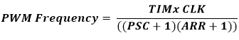
The maximum duty cycle count will be equal to the value that will be set in the timer auto-reload register, TIMx_ARR. In my example, I set PSC zero and ARR 1599 and so now you can see why the PWM frequency is 45 kHz. TIM1_ARR and TIM8_ARR registers are set 1599. Thus 100% duty cycle equals 1599 count, 50% duty cycle equals 800 counts and so forth. As said before, PWM is achieved by comparing counts in the TIMx_CCRn and TIMx_CNT registers. All channels of a timer will have the same PWM frequency but their duty cycles may be different.
The following lines of code set these parameters.
set_TIM1_counting_direction(up_counting);
TIM1_ARR = 1599;
TIM1_PSC = 0;
Then the following code states PWM parameters. PWM mode simply states whether or not to generate inverted PWM. The code also states which PWM channel to use and what should be its polarity. Finally it enables some controls to enable PWM generation.
set_TIM1_OC1_compare_mode(PWM_mode_1);
set_TIM1_CC1_state_and_polarity(enable, active_high);
enable_TIM1_main_output(true);
set_TIM1_CC_preload_control(true);
set_TIM1_auto_reload_preload_mode(true);
For PWM modes interrupts are not necessary as PWM generation is an independent process. To control PWM duty cycle, we only need to load values to TIMx_CCRn, anything between 0 to TIMx_ARR value.
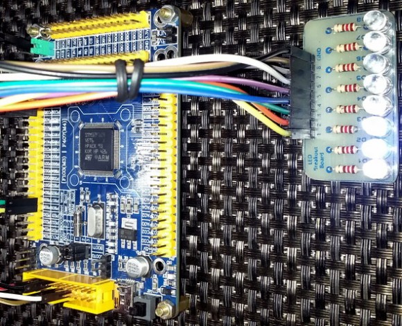
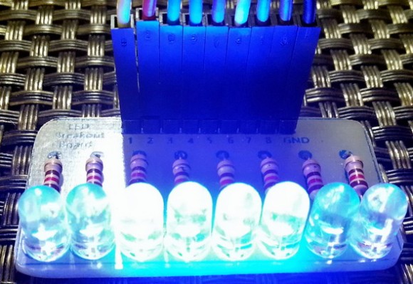
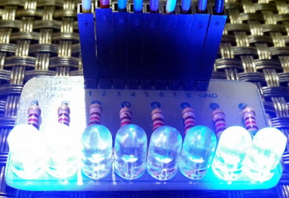
The following hardware setup is used:
The code simply brightens and dims eight LEDs connected to timer PWM channels.
#include "TIM_common.h"
#include "TIM1.h"
#include "TIM8.h"
#include "GPIO.h"
#include "AFIO.h"
void setup();
void setup_IO();
void setup_TIM1();
void setup_TIM8();
void main()
{
unsigned int duty = 0;
setup();
while(1)
{
while(duty < 1600)
{
TIM1_CCR1 = duty;
TIM1_CCR2 = duty;
TIM1_CCR3 = duty;
TIM1_CCR4 = duty;
TIM8_CCR1 = duty;
TIM8_CCR2 = duty;
TIM8_CCR3 = duty;
TIM8_CCR4 = duty;
duty++;
delay_ms(4);
}
while(duty > 0)
{
TIM1_CCR1 = duty;
TIM1_CCR2 = duty;
TIM1_CCR3 = duty;
TIM1_CCR4 = duty;
TIM8_CCR1 = duty;
TIM8_CCR2 = duty;
TIM8_CCR3 = duty;
TIM8_CCR4 = duty;
duty--;
delay_ms(4);
}
};
}
void setup()
{
setup_IO();
setup_TIM1();
setup_TIM8();
}
void setup_IO()
{
AFIO_enable(true);
AFIO_remap(TIM1_not_remapped);
enable_GPIOA(true);
setup_GPIOA(8, (AFIO_PP_output | output_mode_high_speed));
setup_GPIOA(9, (AFIO_PP_output | output_mode_high_speed));
setup_GPIOA(10, (AFIO_PP_output | output_mode_high_speed));
setup_GPIOA(11, (AFIO_PP_output | output_mode_high_speed));
enable_GPIOC(true);
setup_GPIOC(6, (AFIO_PP_output | output_mode_high_speed));
setup_GPIOC(7, (AFIO_PP_output | output_mode_high_speed));
setup_GPIOC(8, (AFIO_PP_output | output_mode_high_speed));
setup_GPIOC(9, (AFIO_PP_output | output_mode_high_speed));
}
void setup_TIM1()
{
enable_TIM1(true);
enable_TIM1_counter(false);
set_TIM1_counting_direction(up_counting);
TIM1_ARR = 1599;
TIM1_PSC = 0;
set_TIM1_OC1_compare_mode(PWM_mode_1);
set_TIM1_OC2_compare_mode(PWM_mode_1);
set_TIM1_OC3_compare_mode(PWM_mode_2);
set_TIM1_OC4_compare_mode(PWM_mode_2);
set_TIM1_CC1_state_and_polarity(enable, active_high);
set_TIM1_CC2_state_and_polarity(enable, active_high);
set_TIM1_CC3_state_and_polarity(enable, active_high);
set_TIM1_CC4_state_and_polarity(enable, active_high);
enable_TIM1_main_output(true);
set_TIM1_CC_preload_control(true);
set_TIM1_auto_reload_preload_mode(true);
enable_TIM1_counter(true);
}
void setup_TIM8()
{
enable_TIM8(true);
enable_TIM8_counter(false);
set_TIM8_counting_direction(down_counting);
TIM8_ARR = 1599;
TIM8_PSC = 0;
set_TIM8_OC1_compare_mode(PWM_mode_1);
set_TIM8_OC2_compare_mode(PWM_mode_1);
set_TIM8_OC3_compare_mode(PWM_mode_2);
set_TIM8_OC4_compare_mode(PWM_mode_2);
set_TIM8_CC1_state_and_polarity(enable, active_low);
set_TIM8_CC2_state_and_polarity(enable, active_low);
set_TIM8_CC3_state_and_polarity(enable, active_low);
set_TIM8_CC4_state_and_polarity(enable, active_low);
enable_TIM8_main_output(true);
set_TIM8_CC_preload_control(true);
set_TIM8_auto_reload_preload_mode(true);
enable_TIM8_counter(true);
}
Demo video link: https://www.youtube.com/watch?v=IwfpD67HUMQ.
Advance Timer Complementary PWM Generation Example
We already know that advance timers have the ability to generate complementary/opposite PWM waveforms. Such PWMs have many applications in power electronics sector. Motor control, inverters and DC-DC converters are a few good examples. In any advance timer there are three pairs of complementary PWM channels denoted as CHx and CHxN. The N signifies the inverted characteristic of that channel. Additionally there are options to add dead-time between these complementary waveforms and do some other advanced tasks.
Dead time automatically adds a delay between waveform transitions. Consider a half-bridge MOSFET configuration. Surely you’ll never want to turn on both MOSFETs during transitions as it will lead to a temporary short circuit between source and ground, and also lead to unnecessary heating of the MOSFETs. By applying dead-time this can be avoided. Luckily STM32 advance timers have this feature.
In terms of programming, complementary PWM generation is not so much dissimilar to ordinary PWM generation. Each and every setup is same except in the case of complementary PWM, we need to enable complementary channels and setup dead-time setting if needed.
In this example only one complementary pair (CH1 and CH1N) of timer 1 is used. Note that TIM1_CCR1 is responsible for the PWM duty cycle of both of these outputs. You’ll notice one LED will brighten complementarily to another. The effect of applying dead-time will be visible when you observe the waveforms.
The hardware setup is like this:
#include "TIM_common.h"
#include "TIM1.h"
#include "GPIO.h"
#include "AFIO.h"
void setup();
void setup_IO();
void setup_TIM1();
void main()
{
unsigned int duty = 0;
setup();
while(1)
{
while(duty < 1600)
{
TIM1_CCR1 = duty;
duty++;
delay_ms(1);
}
while(duty > 0)
{
TIM1_CCR1 = duty;
duty--;
delay_ms(1);
}
};
}
void setup()
{
setup_IO();
setup_TIM1();
}
void setup_IO()
{
AFIO_enable(true);
AFIO_remap(TIM1_not_remapped);
enable_GPIOA(true);
setup_GPIOA(8, (AFIO_PP_output | output_mode_high_speed));
enable_GPIOB(true);
setup_GPIOB(13, (AFIO_PP_output | output_mode_high_speed));
}
void setup_TIM1()
{
enable_TIM1(true);
enable_TIM1_counter(false);
set_TIM1_counting_direction(up_counting);
TIM1_ARR = 1599;
TIM1_PSC = 0;
set_TIM1_OC1_compare_mode(PWM_mode_1);
set_TIM1_CC1_state_and_polarity(enable, active_low);
set_TIM1_CC1_complementary_output_state_and_polarity(enable, active_low);
set_TIM1_off_state_selection_for_run_mode(enable);
set_TIM1_dead_time(77);
enable_TIM1_main_output(true);
set_TIM1_CC_preload_control(true);
set_TIM1_auto_reload_preload_mode(true);
enable_TIM1_counter(true);
}
Demo video link: https://www.youtube.com/watch?v=wfwlfv2-_uY.
Input Capture
Input capture is an added functionality for a timer module and is also available in most modern micros. Again except the basic timers, all STM32 timers can be used for input capture. With this mode we can measure pulse width/duty cycle, frequency of a waveform and count pulses. The concept behind input capture is same in all micros and in STM32 micros this is indifferent. Incoming waveform is sensed by an input pin. The edge transition (rising/falling edge) of the incoming waveform is detected and the current value of timer counter related to the capture pin is saved in the corresponding capture/compare register, TIMx_CCRx. An interrupt/DMA request is then generated to notify capture process completion.
Input capture is also another example where you do not have MikroC built-in library to help you out. Thus we need to code on our own. Just as with output compare mode, we need to deal with a few register sets.
To begin with, we need to look back into TIMx_CCMRx registers. This time we specifically need the second rows of these registers since these are what we will be needing for input capture mode.
We already know that CCxS bits select mode of operation of timer I/O channels. Thus for input capture these bits can’t be both zeroes. Be sure of the channel you wish to use and be sure of these bit settings. ICxPSC bits set input prescaler. Finally ICxF bits configure input filter sampling length. These together help us to truly determine the actual logic state of an incoming waveform that is spiky or somewhat noisy.
We also need to set which channel we are going to use and which edge to detect. These are done by setting the bits in TIMx_CCER registers. Remember these registers are different for advanced and general purpose timers.
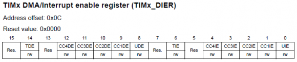
To trigger interrupts/DMA requests we need to set TIMx_DIER register bits. Most timers have one interrupt vector address. There are flags in the Timer Status resgiters, TIMx_SR that are set by hardware to notify which interrupts have occurred. Advance timers have more than one interrupt vector and so be aware of such.
During a capture event TIMx_CCRx registers capture/store the current value of TIMx_CNT register. In this way we get a time-based reference of an input capture event. Comparing two such even will enable us to determine pulse width or frequency of a waveform.
Code Examples
Input Capture Example
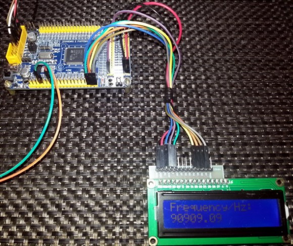
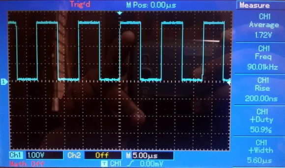
In this example we will employ the input capture feature of STM32 timers to measure the frequency of an incoming waveform. For this task we will need two components of a timer – input capture component to detect waveform and a time base to keep track of time. The example is made out as such that another timer will provide the waveform for capture. Timer 3 is used to generate 90 kHz PWM having roughly equal mark to space ratio. Timer 2 is used to capture this waveform and determine its frequency.
For input capture timer channels need to be specified as inputs, additionally pull resistors may be use. The code for timer 2 setup can be realized as two parts. One part sets it as a time base generator while the other sets up input capture properties. Let us have look at this setup:
TIM2_ARR = 0xFFFF;
TIM2_PSC = 71;
set_TIM2_counting_direction(up_counting);
set_TIM2_clock_division(clock_division_tCK_INT);
set_TIM2_CC1_selection(CC1_input_IC1_on_TI1);
set_TIM2_CC1_state_and_polarity(enable, rising_edge);
set_TIM2_IC1_input_prescalar(0);
set_TIM2_IC1_filter(0);
Firstly the PSC value divides the 72 MHz timer input clock to 1MHz. The external input is not scaled or filtered by any factor for simplicity. The input channel to be used is selected and set to detect rising edges of the incoming waveform.
Timer 2 interrupt occurs when either timer 2overflows or a capture event occurs. Each time a rising edge is detected, capture interrupt flag is set in the timer status register, TIMx_SR and the current timer count in TIMx_CNT register is stored in the corresponding TIMx_CCRn register. The time between two rising edges is captured and calculated in the interrupt sub-routine. Sometimes the time between these two edges may get long and so the timer may overflow. This is checked by the update interrupt flag. Using the time difference between two edge captures we can compute time period and thereby frequency. The following piece of code does this:
end_time = TIM2_CCR1;
pulse_ticks = ((overflow_count << 16) - start_time + end_time);
start_time = end_time;
The segment of the code shown below actually computes input waveform frequency.
f = (float)pulse_ticks;
f = (1000000 / f);
After completing calculations, a LCD display shows the value of frequency.
The following hardware setup is used for this demo:
#include "TIM_common.h"
#include "TIM2.h"
#include "TIM3.h"
#include "AFIO.h"
#include "GPIO.h"
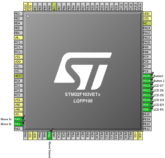
sbit LCD_RS at GPIOD_ODR.B8;
sbit LCD_EN at GPIOD_ODR.B9;
sbit LCD_D4 at GPIOD_ODR.B10;
sbit LCD_D5 at GPIOD_ODR.B11;
sbit LCD_D6 at GPIOD_ODR.B12;
sbit LCD_D7 at GPIOD_ODR.B13;
unsigned int overflow_count = 0;
unsigned long pulse_ticks = 0;
unsigned long start_time = 0;
unsigned long end_time = 0;
float f = 0.0;
void setup();
void setup_IO();
void setup_TIM2();
void setup_TIM3();
void TIM2_ISR()
iv IVT_INT_TIM2
ics ICS_AUTO
{
if(TIM2_SRbits.UIF == 1)
{
TIM2_SRbits.UIF = 0;
overflow_count++;
}
if(TIM2_SRbits.CC1IF == 1)
{
TIM2_SRbits.CC1IF = 0;
end_time = TIM2_CCR1;
pulse_ticks = ((overflow_count << 16) - start_time + end_time);
start_time = end_time;
overflow_count = 0;
}
}
void main()
{
char txt[15];
setup();
while(1)
{
f = (float)pulse_ticks;
f = (1000000 / f);
lcd_out(2, 1, " ");
FloatToStr(f, txt);
lcd_out(2, 1, txt);
delay_ms(600);
};
}
void setup()
{
setup_IO();
setup_TIM2();
setup_TIM3();
Lcd_Init();
Lcd_Cmd(_LCD_CLEAR);
Lcd_Cmd(_LCD_CURSOR_OFF);
Lcd_Out(1, 1, "Frequency/Hz:");
}
void setup_IO()
{
AFIO_enable(true);
AFIO_remap(TIM2_not_remapped);
AFIO_remap(TIM3_not_remapped);
enable_GPIOA(true);
setup_GPIOA(0, digital_input);
enable_pull_down_GPIOA(0);
setup_GPIOA(6, (AFIO_PP_output | output_mode_high_speed));
enable_GPIOD(true);
setup_GPIOD(8, (GPIO_PP_output | output_mode_low_speed));
setup_GPIOD(9, (GPIO_PP_output | output_mode_low_speed));
setup_GPIOD(10, (GPIO_PP_output | output_mode_low_speed));
setup_GPIOD(11, (GPIO_PP_output | output_mode_low_speed));
setup_GPIOD(12, (GPIO_PP_output | output_mode_low_speed));
setup_GPIOD(13, (GPIO_PP_output | output_mode_low_speed));
}
void setup_TIM2()
{
enable_TIM2(true);
enable_TIM2_counter(false);
TIM2_ARR = 0xFFFF;
TIM2_PSC = 71;
set_TIM2_counting_direction(up_counting);
set_TIM2_clock_division(clock_division_tCK_INT);
set_TIM2_CC1_selection(CC1_input_IC1_on_TI1);
set_TIM2_CC1_state_and_polarity(enable, rising_edge);
set_TIM2_IC1_input_prescalar(0);
set_TIM2_IC1_filter(0);
enable_TIM2_CC1_interrupt(true);
enable_TIM2_update_interrupt(true);
NVIC_IntEnable(IVT_INT_TIM2);
EnableInterrupts();
enable_TIM2_counter(true);
}
void setup_TIM3()
{
enable_TIM3(true);
enable_TIM3_counter(false);
set_TIM3_counting_direction(up_counting);
TIM3_ARR = 799;
TIM3_PSC = 0;
set_TIM3_OC1_compare_mode(PWM_mode_1);
set_TIM3_CC1_state_and_polarity(enable, active_low);
enable_TIM3_counter(true);
TIM3_CCR1 = 400;
}
Demo video link: https://www.youtube.com/watch?v=cIz887UzTk8.
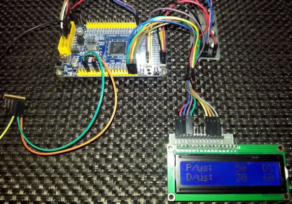
Pulse Width Measurement Example
This is another useful application of input capture mode. Using two I/O pins simplify coding. One pin is set to capture rising edges while the other is configured to capture falling edges. Just like the previous example we need to detect the time difference between two successive capture events. Technically this example is an extension of the previous example.
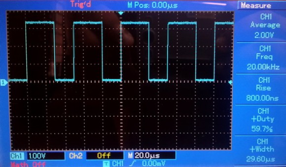
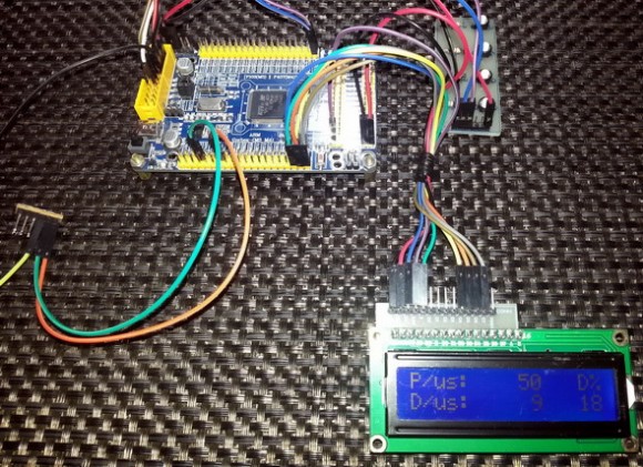
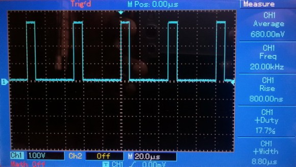
In this example, timer 3 is used as a PWM generator. The PWM waveform will have a frequency of 20 kHz. Two input capture channels are used to detect the two different edges of this PWM. The time difference between a rising edge and a falling edge gives the mark time and the time difference between two rising/falling edges gives the time period of the PWM waveform. Two push buttons connected to GPIOD pins 14 and 15 are used to change the duty cycle of the PWM waveform.
The hardware setup looks like this:
 #include “TIM_common.h”
#include "TIM2.h"
#include "TIM3.h"
#include "AFIO.h"
#include "GPIO.h"
sbit LCD_RS at GPIOD_ODR.B8;
sbit LCD_EN at GPIOD_ODR.B9;
sbit LCD_D4 at GPIOD_ODR.B10;
sbit LCD_D5 at GPIOD_ODR.B11;
sbit LCD_D6 at GPIOD_ODR.B12;
sbit LCD_D7 at GPIOD_ODR.B13;
unsigned int second_rise = 0;
unsigned int start_time = 0;
unsigned int end_time = 0;
unsigned int d = 0;
unsigned int t = 0;
void setup();
void setup_IO();
void setup_TIM2();
void setup_TIM3();
void TIM2_ISR()
iv IVT_INT_TIM2
ics ICS_AUTO
{
if(TIM2_SRbits.CC1IF == 1)
{
TIM2_SRbits.CC1IF = 0;
start_time = TIM2_CCR1;
if(start_time > second_rise)
{
t = (start_time - second_rise);
}
else
{
t = (0xFFFF - start_time + second_rise);
}
}
if(TIM2_SRbits.CC2IF == 1)
{
TIM2_SRbits.CC2IF = 0;
end_time = TIM2_CCR2;
if(start_time < end_time)
{
d = (end_time - start_time);
}
else
{
d = (0xFFFF - end_time + start_time);
}
}
second_rise = start_time;
}
void main()
{
unsigned char duty_cycle = 0;
signed int pwm = 100;
char txt[15];
setup();
while(1)
{
if(get_GPIOD_pin_state(14))
{
pwm += 50;
}
if(pwm >= 3550)
{
pwm = 3550;
}
if(get_GPIOD_pin_state(15))
{
pwm -= 50;
}
if(pwm <= 50)
{
pwm = 50;
}
TIM3_CCR1 = pwm;
duty_cycle = (((float)d / (float)t) * 100);
lcd_out(1, 7, " ");
WordToStr(t, txt);
lcd_out(1, 7, txt);
lcd_out(2, 7, " ");
WordToStr(d, txt);
lcd_out(2, 7, txt);
ByteToStr(duty_cycle, txt);
lcd_out(2, 14, txt);
delay_ms(600);
};
}
void setup()
{
setup_IO();
setup_TIM2();
setup_TIM3();
Lcd_Init();
Lcd_Cmd(_LCD_CLEAR);
Lcd_Cmd(_LCD_CURSOR_OFF);
lcd_out(1, 1, "P/us:");
lcd_out(2, 1, "D/us:");
lcd_out(1, 15, "D%");
}
void setup_IO()
{
AFIO_enable(true);
AFIO_remap(TIM2_not_remapped);
enable_GPIOA(true);
setup_GPIOA(0, digital_input);
enable_pull_down_GPIOA(0);
setup_GPIOA(1, digital_input);
enable_pull_down_GPIOA(1);
setup_GPIOA(6, (AFIO_PP_output | output_mode_high_speed));
enable_GPIOD(true);
setup_GPIOD(8, (GPIO_PP_output | output_mode_low_speed));
setup_GPIOD(9, (GPIO_PP_output | output_mode_low_speed));
setup_GPIOD(10, (GPIO_PP_output | output_mode_low_speed));
setup_GPIOD(11, (GPIO_PP_output | output_mode_low_speed));
setup_GPIOD(12, (GPIO_PP_output | output_mode_low_speed));
setup_GPIOD(13, (GPIO_PP_output | output_mode_low_speed));
setup_GPIOD(14, input_without_pull_resistors);
setup_GPIOD(15, input_without_pull_resistors);
}
void setup_TIM2()
{
enable_TIM2(true);
enable_TIM2_counter(false);
TIM2_ARR = 0xFFFF;
TIM2_PSC = 71;
set_TIM2_counting_direction(up_counting);
set_TIM2_clock_division(clock_division_tCK_INT);
set_TIM2_CC1_selection(CC1_input_IC1_on_TI1);
set_TIM2_CC2_selection(CC2_input_IC2_on_TI1);
set_TIM2_CC1_state_and_polarity(enable, rising_edge);
set_TIM2_CC2_state_and_polarity(enable, falling_edge);
set_TIM2_IC1_input_prescalar(0);
set_TIM2_IC2_input_prescalar(0);
set_TIM2_IC1_filter(0);
set_TIM2_IC2_filter(0);
enable_TIM2_CC1_interrupt(true);
enable_TIM2_CC2_interrupt(true);
NVIC_IntEnable(IVT_INT_TIM2);
EnableInterrupts();
enable_TIM2_counter(true);
}
void setup_TIM3()
{
enable_TIM3(true);
enable_TIM3_counter(false);
set_TIM3_counting_direction(up_counting);
TIM3_ARR = 3599;
TIM3_PSC = 0;
set_TIM3_OC1_compare_mode(PWM_mode_2);
set_TIM3_CC1_state_and_polarity(enable, active_low);
enable_TIM3_counter(true);
}
Demo video link: https://www.youtube.com/watch?v=BJI5K0yBm6s.
One Pulse Mode Example
One pulse mode is a combination of both input capture and output compare modes. In this mode a timer behaves like a monostable multivibrator (A.K.A one shot timer). It will fire a pulse of a given width and then go to idle state. This is another feature that is uncommon to most other micros.
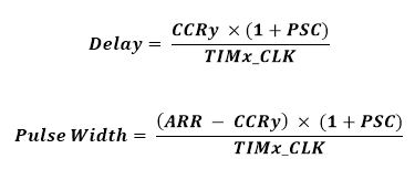
There are two timings to consider when using one pulse mode. First is the delay after which the pulse will be generated and second is the pulse width. These are calculated as follows:
The following code sets up timer 2 for one pulse mode:
set_TIM2_counting_direction(up_counting);
set_TIM2_clock_division(clock_division_tCK_INT);
set_TIM2_CC1_selection(CC1_input_IC1_on_TI1);
set_TIM2_CC1_state_and_polarity(enable, rising_edge);
set_TIM2_CC2_selection(CC2_output);
set_TIM2_CC2_state_and_polarity(enable, active_high);
set_TIM2_OC2_compare_mode(PWM_mode_2);
set_TIM2_trigger_source(Filtered_Timer_Input_1);
set_TIM2_slave_selection(trigger_mode);
TIM2_ARR = 60000;
TIM2_PSC = 0x0000;
TIM2_CCR2 = 20;
The code configures an input capture c and an output compare channel. It sets up their properties. The different thing in this code from the others is the slave selection and the trigger source selection. Trigger mode needs to be selected for one pulse mode.
Note the values of ARR, PSC and CCR2 registers. With these values we will get a pulse of 833µs after a delay of about 280ns.
In my example I used a button to trigger the timer and an LED to show the output. When the button is pressed, the LED will briefly light and then extinguish, showing one shot characteristics.
The hardware setup for this example is like this:
#include "TIM_common.h"
#include "TIM2.h"
#include "AFIO.h"
#include "GPIO.h"
void setup();
void setup_IO();
void setup_TIM2();
void main()
{
setup();
while(1)
{
};
}
void setup()
{
setup_IO();
setup_TIM2();
}
void setup_IO()
{
AFIO_enable(true);
AFIO_remap(TIM2_not_remapped);
enable_GPIOA(true);
setup_GPIOA(0, digital_input);
enable_pull_down_GPIOA(0);
setup_GPIOA(1, (AFIO_PP_output | output_mode_high_speed));
}
void setup_TIM2()
{
enable_TIM2(true);
enable_TIM2_counter(false);
set_TIM2_counting_direction(up_counting);
set_TIM2_clock_division(clock_division_tCK_INT);
set_TIM2_CC1_selection(CC1_input_IC1_on_TI1);
set_TIM2_CC1_state_and_polarity(enable, rising_edge);
set_TIM2_CC2_selection(CC2_output);
set_TIM2_CC2_state_and_polarity(enable, active_high);
set_TIM2_OC2_compare_mode(PWM_mode_2);
set_TIM2_trigger_source(Filtered_Timer_Input_1);
set_TIM2_slave_selection(trigger_mode);
TIM2_ARR = 60000;
TIM2_PSC = 0x0000;
TIM2_CCR2 = 20;
enable_TIM2_counter(true);
}
Demo video link: https://www.youtube.com/watch?v=-qctr7AVrrI.
Epilogue
Oh that was too much for one post I guess. Nearly one month of hard work and continuous studies compiled here. I believe it is my longest post so far. Previously the post on STM32 ADC was the longest. I tried my best to give the most out of STM32 timers. A total of nine examples I suppose covered most of the STM32 timer stuffs one can desire. DMA-based operations were skipped for future just as like other posts. I would suggest readers to read the STM32 Timer Overview application note (AN4013) from ST instead of going through the reference manuals:
http://www.st.com/web/en/resource/technical/document/application_note/DM00042534.pdf
This app note described timers pretty much simply than reference manuals. I’m not suggesting to avoid the reference manuals. They’ll be needed for register overviews and other tasks.
References:
- STM32 Reference Manual RM0008.
- STM32 Timer Overview AN4013.
Files: STM32 Timers.
Happy coding.
Author: Shawon M. Shahryiar
https://www.facebook.com/groups/microarena
https://www.facebook.com/MicroArena 01.11.2015
The post STM32 Timers appeared first on Embedded Lab.