Obviously the first example is based on MikroC’s ADC library. MikroC compiler provided an easy to use ADC library. With this library you can do basic ADC readings and set up ADC units easily with minimum coding. MikroC’s built-in ADC library functions are as follows:
MikroC IDE’s help section explains the purpose of these function.
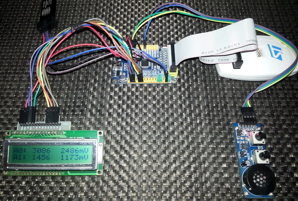
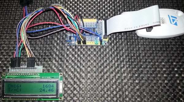
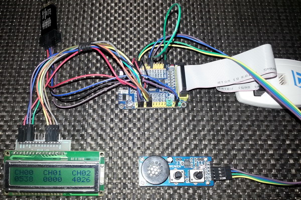
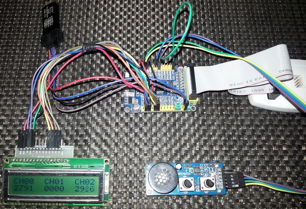
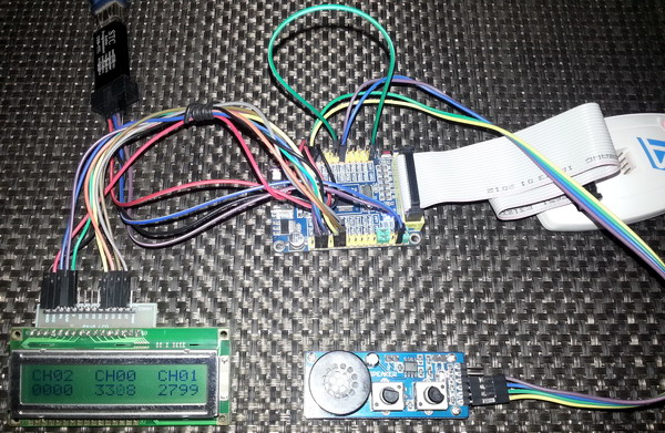
In this demo I just showed how to use MikroC’s built-in ADC library functions to initialize, get average ADC counts from two ADC channels and show both ADC counts and voltage levels of each channel on a LCD display. Just a piece of cake. Not much to explain. ![MikroC Library (2)]()
![MikroC Library (1)]() Demo video link: https://www.youtube.com/watch?v=TwMTOLkWt-Q.
Demo video link: https://www.youtube.com/watch?v=TwMTOLkWt-Q.
Analogue Watchdog
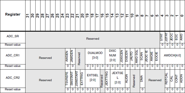
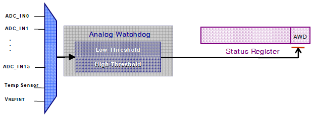
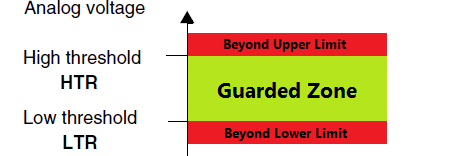
One of the cool feature of STM32 micros is the Analogue Watchdog (AWD) unit. In traditional micros, a programmer needs to add an if-else clause to monitor if the ADC readouts are within some predefined limits. There are, therefore, some coding and resource involved. The AWD unit of STM32 micros can monitor if an ADC channel or all ADC channels are exceeding or within predefine upper and lower ADC count limits. In this way we can effectively set an analogue voltage level window for the ADC block. Thus this unit allows users to easily implement signal level monitors, zero-crossing detectors, analogue comparators and many other stuffs. Thanks to ST for hardcoding this useful feature with the ADC block. ![ADC AWD Unit]() The upper and lower limit 12-bit values are stored in the High Threshold (HTR) and Lower Threshold (LTR) registers respectively. When the analogue input to be monitored is within these limits or inside guarded zone the AWD unit stays idle. When it is the other way around, the AWD wakes up. An AWD event interrupt can be generated if the AWD interrupt is enabled.
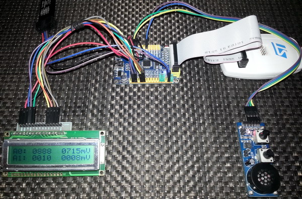
The upper and lower limit 12-bit values are stored in the High Threshold (HTR) and Lower Threshold (LTR) registers respectively. When the analogue input to be monitored is within these limits or inside guarded zone the AWD unit stays idle. When it is the other way around, the AWD wakes up. An AWD event interrupt can be generated if the AWD interrupt is enabled. ![AWD]() Setting AWDSGL bit, AWDEN bit and JAWDEN bit in the ADC_CR1 select which channel types the AWD unit would monitor. The demo code for AWD is just same as the previous one but this time the AWD is also used to monitor all regular ADC channels. If the ADC readings exceed the guarded zone of 400 to 3695 ADC counts, the AWD fires. This mark starts to blink a LED connected to PC13, indicating an AWD event.
Setting AWDSGL bit, AWDEN bit and JAWDEN bit in the ADC_CR1 select which channel types the AWD unit would monitor. The demo code for AWD is just same as the previous one but this time the AWD is also used to monitor all regular ADC channels. If the ADC readings exceed the guarded zone of 400 to 3695 ADC counts, the AWD fires. This mark starts to blink a LED connected to PC13, indicating an AWD event.
sbit LCD_RS at GPIOB_ODR.B1;
sbit LCD_EN at GPIOB_ODR.B2;
sbit LCD_D4 at GPIOB_ODR.B12;
sbit LCD_D5 at GPIOB_ODR.B13;
sbit LCD_D6 at GPIOB_ODR.B14;
sbit LCD_D7 at GPIOB_ODR.B15;
#define high_level 3695
#define low_level 400
void setup();
unsigned int adc_avg(unsigned char no_of_samples, unsigned char channel);
void lcd_print(unsigned char x_pos, unsigned char y_pos, unsigned int value);
float map(float v, float x_min, float x_max, float y_min, float y_max);
void main()
{
unsigned char s = 0;
register unsigned int adc_data = 0;
float v = 0.0;
setup();
while(1)
{
for(s = 0; s < 2; s++)
{
adc_data = adc_avg(20, s);
v = map(adc_data, 0, 4095, 0, 3300);
lcd_print(5, (s + 1), adc_data);
lcd_print(11, (s + 1), v);
}
if(ADC1_SRbits.AWD == 1)
{
GPIOC_ODRbits.ODR13 ^= 1;
ADC1_SRbits.AWD = 0;
}
else
{
GPIOC_ODRbits.ODR13 = 0;
}
delay_ms(400);
};
}
void setup()
{
GPIO_Clk_Enable(&GPIOA_BASE);
GPIO_Clk_Enable(&GPIOB_BASE);
GPIO_Clk_Enable(&GPIOC_BASE);
GPIO_Config(&GPIOA_BASE, (_GPIO_PINMASK_0 | _GPIO_PINMASK_1), (_GPIO_CFG_MODE_ANALOG | _GPIO_CFG_PULL_NO));
GPIO_Config(&GPIOC_BASE, _GPIO_PINMASK_13, (_GPIO_CFG_MODE_OUTPUT | _GPIO_CFG_SPEED_MAX | _GPIO_CFG_OTYPE_PP));
ADC1_init();
ADC1_LTR = low_level;
ADC1_HTR = high_level;
ADC1_CR1bits.AWDEN = 1;
LCD_Init();
LCD_Cmd(_LCD_CLEAR);
LCD_Cmd(_LCD_CURSOR_OFF);
lcd_out(1, 1, "A0:");
lcd_out(2, 1, "A1:");
lcd_out(1, 15, "mV");
lcd_out(2, 15, "mV");
}
unsigned int adc_avg(unsigned char no_of_samples, unsigned char channel)
{
register unsigned long avg = 0;
unsigned char samples = no_of_samples;
while(samples > 0)
{
avg += ADC1_Get_Sample(channel);
samples--;
}
avg /= no_of_samples;
return avg;
}
void lcd_print(unsigned char x_pos, unsigned char y_pos, unsigned int value)
{
unsigned char tmp = 0;
tmp = (value / 1000);
lcd_chr(y_pos, x_pos, (tmp + 48));
tmp = ((value / 100) % 10);
lcd_chr_cp((tmp + 48));
tmp = ((value / 10) % 10);
lcd_chr_cp((tmp + 48));
tmp = (value % 10);
lcd_chr_cp((tmp + 48));
}
float map(float v, float x_min, float x_max, float y_min, float y_max)
{
return (y_min + (((y_max - y_min)/(x_max - x_min)) * (v - x_min)));
}
![AWD (2)]()
![AWD (1)]() Demo video link: https://www.youtube.com/watch?v=xMDIaEq-Q8o.
Demo video link: https://www.youtube.com/watch?v=xMDIaEq-Q8o.
Interrupt-Driven Single Channel Continuous Conversion Mode
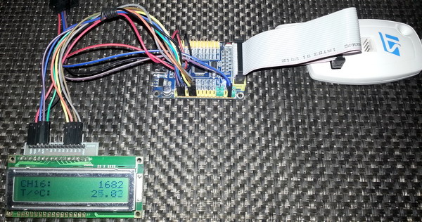
Many of us may overlook one feature of STM32 micros and that is no other than the presence of an on-chip temperature sensor. All STM32 micros have this sensor. Although it is not recommended for precise temperature measurements, it can be used to estimate PCB or surrounding temperatures around a STM32 micro. The single channel continuous conversion mode is one of the most basic ADC mode. In this mode, once an ADC is triggered a single channel associated with it is continuously converted. In this demo, the single channel is the temperature sensor. The end of conversion interrupt is used to extract ADC conversion result after a conversion finishes. In this way, the CPU is not busy waiting for the ADC to finish conversion. After the end of a conversion, the entire process is repeated and this makes it continuous. From this example onwards you’ll mostly see me incorporating header file from my own SPL with my codes. Take this into account. In the reference manual for STM32F10x series, there’s an entire section dedicated to this temperature sensor. I suggest that you check it out first before trying to understand the code example.
#include "ADC.h"
#include "GPIO.h"
#define V25 1430
#define T_offset 17.5
sbit LCD_RS at GPIOB_ODR.B1;
sbit LCD_EN at GPIOB_ODR.B2;
sbit LCD_D4 at GPIOB_ODR.B12;
sbit LCD_D5 at GPIOB_ODR.B13;
sbit LCD_D6 at GPIOB_ODR.B14;
sbit LCD_D7 at GPIOB_ODR.B15;
register unsigned int adc_data = 0;
const char symbol[8] = {0x00, 0x06, 0x09, 0x09, 0x06, 0x00, 0x00, 0x00};
void setup();
void GPIO_init();
void ADC_init();
void CustomChar(unsigned char y_pos, unsigned char x_pos);
void lcd_print(unsigned char x_pos, unsigned char y_pos, unsigned int value, unsigned char disp_type);
float map(float v, float x_min, float x_max, float y_min, float y_max);
void ADC_ISR()
iv IVT_INT_ADC1_2
ics ICS_AUTO
{
adc_data = (ADC1_DR & 0x0FFF);
bit_set(GPIOC_ODR, 13);
}
void main()
{
register float t = 0.0;
setup();
while(1)
{
t = map(adc_data, 0, 4095, 0, 3300);
t = (((V25 - t) / 4.3) + 25);
t -= T_offset;
t *= 100;
if(t <= 0)
{
t = 0;
}
if(t >= 9999)
{
t = 9999;
}
lcd_print(13, 1, adc_data, 1);
lcd_print(12, 2, t, 0);
bit_clr(GPIOC_ODR, 13);
delay_ms(90);
};
}
void setup()
{
GPIO_init();
ADC_init();
LCD_Init();
LCD_Cmd(_LCD_CLEAR);
LCD_Cmd(_LCD_CURSOR_OFF);
lcd_out(1, 1, "CH16:");
lcd_out(2, 1, "T/ C:");
CustomChar(2, 3);
}
void GPIO_init()
{
enable_GPIOB(enable);
enable_GPIOC(enable);
pin_configure_high(GPIOC_CRH, 13, (GPIO_PP_output | output_mode_low_speed));
}
void ADC_init()
{
ADC1_Enable();
clr_ADC1_settings();
set_ADC_mode(independent_mode);
set_ADC1_data_alignment(right_alignment);
set_ADC1_scan_conversion_mode(disable);
set_ADC1_continuous_conversion_mode(enable);
set_ADC1_external_trigger_regular_conversion_edge(SWSTART_trigger);
set_ADC1_regular_number_of_conversions(1);
set_ADC1_sample_time(sample_time_13_5_cycles, 16);
set_ADC1_regular_sequence(1, 16);
set_ADC1_reference_and_temperature_sensor(enable);
set_ADC1_regular_end_of_conversion_interrupt(enable);
NVIC_IntEnable(IVT_INT_ADC1_2);
EnableInterrupts;
ADC1_calibrate();
start_ADC1();
}
void CustomChar(unsigned char y_pos, unsigned char x_pos)
{
unsigned char i = 0;
Lcd_Cmd(64);
for (i = 0; i < 8; i += 1)
{
Lcd_Chr_CP(symbol[i]);
}
Lcd_Cmd(_LCD_RETURN_HOME);
Lcd_Chr(y_pos, x_pos, 0);
}
void lcd_print(unsigned char x_pos, unsigned char y_pos, unsigned int value, unsigned char disp_type)
{
unsigned char tmp = 0;
tmp = (value / 1000);
lcd_chr(y_pos, x_pos, (tmp + 48));
tmp = ((value / 100) % 10);
lcd_chr_cp((tmp + 48));
switch(disp_type)
{
case 0:
{
lcd_chr_cp(46);
break;
}
case 1:
{
break;
}
}
tmp = ((value / 10) % 10);
lcd_chr_cp((tmp + 48));
tmp = (value % 10);
lcd_chr_cp((tmp + 48));
}
float map(float v, float x_min, float x_max, float y_min, float y_max)
{
return (y_min + (((y_max - y_min)/(x_max - x_min)) * (v - x_min)));
}
![Internal Temperature Sensor (1)]()
![Internal Temperature Sensor (2)]() Demo video link: https://www.youtube.com/watch?v=01sV-vgegtk.
Demo video link: https://www.youtube.com/watch?v=01sV-vgegtk.
Interrupt-Driven Single Channel Single Conversion Mode
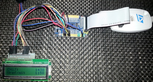
STM32 micros have an internal bandgap voltage reference source. The internal voltage reference source is not used by the ADC unlike other micros. It can, however, be used as a comparator input for zero-crossing detection. It may also be possible to use it to calibrate external readings or the V_Ref+ pin. The single channel single conversion mode is another basic ADC mode. In this mode a single channel (the internal reference source as in this example) is converted once when triggered. A single software trigger is used to invoke one ADC conversion. The end of conversion interrupt is used to notify the completion of ADC conversion and then the ADC stops. The only difference between the previous example and this one is how often the ADC conversion is done.
#include "ADC.h"
#include "GPIO.h"
sbit LCD_RS at GPIOB_ODR.B1;
sbit LCD_EN at GPIOB_ODR.B2;
sbit LCD_D4 at GPIOB_ODR.B12;
sbit LCD_D5 at GPIOB_ODR.B13;
sbit LCD_D6 at GPIOB_ODR.B14;
sbit LCD_D7 at GPIOB_ODR.B15;
register unsigned int adc_data = 0;
void setup();
void GPIO_init();
void ADC_init();
void lcd_print(unsigned char x_pos, unsigned char y_pos, unsigned int value);
float map(float v, float x_min, float x_max, float y_min, float y_max);
void ADC_ISR()
iv IVT_INT_ADC1_2
ics ICS_AUTO
{
adc_data = (ADC1_DR & 0x0FFF);
bit_clr(GPIOC_ODR, 13);
}
void main()
{
register float V = 0;
setup();
while(1)
{
set_ADC1_regular_conversions(enable);
bit_set(GPIOC_ODR, 13);
V = map(adc_data, 0, 4095, 0, 3300);
lcd_print(13, 1, adc_data);
lcd_print(13, 2, V);
delay_ms(90);
};
}
void setup()
{
GPIO_init();
ADC_init();
LCD_Init();
LCD_Cmd(_LCD_CLEAR);
LCD_Cmd(_LCD_CURSOR_OFF);
lcd_out(1, 1, "CH17:");
lcd_out(2, 1, "Vref/mV:");
}
void GPIO_init()
{
enable_GPIOB(enable);
enable_GPIOC(enable);
pin_configure_high(GPIOC_CRH, 13, (GPIO_PP_output | output_mode_low_speed));
}
void ADC_init()
{
ADC1_Enable();
clr_ADC1_settings();
set_ADC_mode(independent_mode);
set_ADC1_data_alignment(right_alignment);
set_ADC1_scan_conversion_mode(disable);
set_ADC1_continuous_conversion_mode(disable);
set_ADC1_external_trigger_regular_conversion_edge(SWSTART_trigger);
set_ADC1_regular_number_of_conversions(1);
set_ADC1_sample_time(sample_time_13_5_cycles, 17);
set_ADC1_regular_sequence(1, 17);
set_ADC1_reference_and_temperature_sensor(enable);
set_ADC1_regular_end_of_conversion_interrupt(enable);
NVIC_IntEnable(IVT_INT_ADC1_2);
EnableInterrupts();
ADC1_calibrate();
start_ADC1();
}
void lcd_print(unsigned char x_pos, unsigned char y_pos, unsigned int value)
{
unsigned char tmp = 0;
tmp = (value / 1000);
lcd_chr(y_pos, x_pos, (tmp + 48));
tmp = ((value / 100) % 10);
lcd_chr_cp((tmp + 48));
tmp = ((value / 10) % 10);
lcd_chr_cp((tmp + 48));
tmp = (value % 10);
lcd_chr_cp((tmp + 48));
}
float map(float v, float x_min, float x_max, float y_min, float y_max)
{
return (y_min + (((y_max - y_min)/(x_max - x_min)) * (v - x_min)));
}
![Internal Reference Source]() Demo video link: https://www.youtube.com/watch?v=BpiCa0ANWVI.
Demo video link: https://www.youtube.com/watch?v=BpiCa0ANWVI.
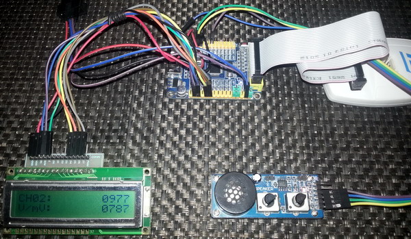
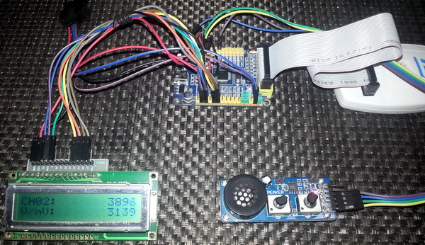
Single Channel Continuous Conversion Mode
This is similar to the third ADC example but this one is based on polling method rather than end of conversion interrupt-based one. This example is another basic example but I would prefer interrupt-based ADC conversion rather than this one as it will slow down other tasks.
#include "ADC.h"
#include "GPIO.h"
sbit LCD_RS at GPIOB_ODR.B1;
sbit LCD_EN at GPIOB_ODR.B2;
sbit LCD_D4 at GPIOB_ODR.B12;
sbit LCD_D5 at GPIOB_ODR.B13;
sbit LCD_D6 at GPIOB_ODR.B14;
sbit LCD_D7 at GPIOB_ODR.B15;
void setup();
void GPIO_init();
void ADC_init();
unsigned int read_ADC1();
void lcd_print(unsigned char x_pos, unsigned char y_pos, unsigned int value);
float map(float v, float x_min, float x_max, float y_min, float y_max);
void main()
{
unsigned int adc_data = 0;
float V = 0.0;
setup();
while(1)
{
bit_set(GPIOC_ODR, 13);
delay_ms(10);
adc_data = read_ADC1();
V = map(adc_data, 0, 4095, 0, 3300);
lcd_print(13, 1, adc_data);
lcd_print(13, 2, V);
bit_clr(GPIOC_ODR, 13);
delay_ms(90);
};
}
void setup()
{
GPIO_init();
ADC_init();
LCD_Init();
LCD_Cmd(_LCD_CLEAR);
LCD_Cmd(_LCD_CURSOR_OFF);
lcd_out(1, 1, "CH02:");
lcd_out(2, 1, "V/mV:");
}
void GPIO_init()
{
enable_GPIOA(enable);
enable_GPIOB(enable);
enable_GPIOC(enable);
pin_configure_low(GPIOA_CRL, 2, (analog_input | input_mode));
pin_configure_high(GPIOC_CRH, 13, (GPIO_PP_output | output_mode_low_speed));
}
void ADC_init()
{
ADC1_Enable();
clr_ADC1_settings();
set_ADC_mode(independent_mode);
set_ADC1_data_alignment(right_alignment);
set_ADC1_scan_conversion_mode(disable);
set_ADC1_continuous_conversion_mode(enable);
set_ADC1_regular_number_of_conversions(1);
set_ADC1_sample_time(sample_time_41_5_cycles, 2);
set_ADC1_regular_sequence(1, 2);
set_ADC1_external_trigger_regular_conversion_edge(SWSTART_trigger);
ADC1_calibrate();
start_ADC1();
}
unsigned int read_ADC1()
{
while(ADC1_SRbits.EOC == 0);
return (ADC1_DR & 0x0FFF);
}
void lcd_print(unsigned char x_pos, unsigned char y_pos, unsigned int value)
{
unsigned char tmp = 0;
tmp = (value / 1000);
lcd_chr(y_pos, x_pos, (tmp + 48));
tmp = ((value / 100) % 10);
lcd_chr_cp((tmp + 48));
tmp = ((value / 10) % 10);
lcd_chr_cp((tmp + 48));
tmp = (value % 10);
lcd_chr_cp((tmp + 48));
}
float map(float v, float x_min, float x_max, float y_min, float y_max)
{
return (y_min + (((y_max - y_min)/(x_max - x_min)) * (v - x_min)));
}
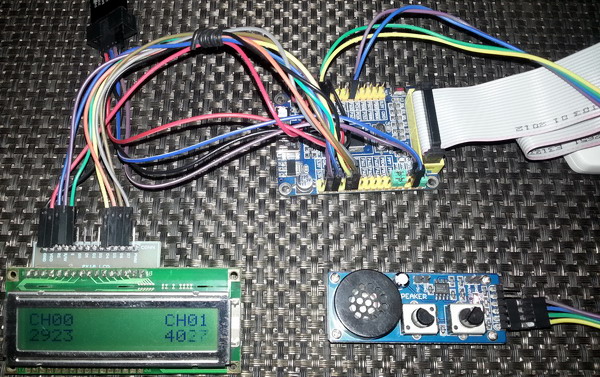
![Single Channel Continuous Conversion Mode (2)]()
![Single Channel Continuous Conversion Mode (1)]() Demo video link: https://www.youtube.com/watch?v=8fh1-rkpFAw.
Demo video link: https://www.youtube.com/watch?v=8fh1-rkpFAw.
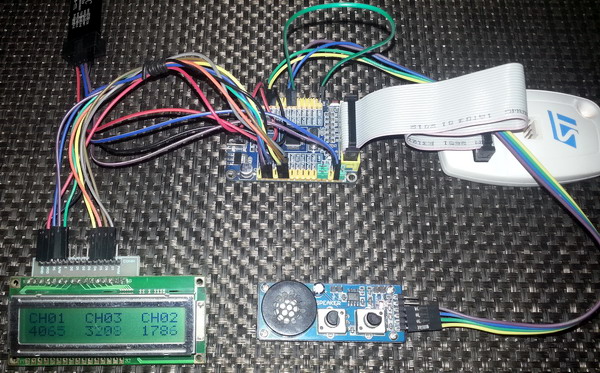
Multi-Single Channel Single Conversion Mode
This example is similar to the 4th example of this post but instead of reading a single channel multiple single channels with different sampling times are read. It is useful when you need to read multiple channels without scanning them.
#include "ADC.h"
#include "GPIO.h"
sbit LCD_RS at GPIOB_ODR.B1;
sbit LCD_EN at GPIOB_ODR.B2;
sbit LCD_D4 at GPIOB_ODR.B12;
sbit LCD_D5 at GPIOB_ODR.B13;
sbit LCD_D6 at GPIOB_ODR.B14;
sbit LCD_D7 at GPIOB_ODR.B15;
void setup();
void GPIO_init();
void ADC_init();
unsigned int read_ADC1(unsigned char channel, unsigned char sample_time);
void lcd_print(unsigned char x_pos, unsigned char y_pos, unsigned int value);
void main()
{
unsigned int ch_a = 0;
unsigned int ch_b = 0;
unsigned int ch_c = 0;
setup();
while(1)
{
ch_a = read_ADC1(1, sample_time_239_5_cycles);
ch_b = read_ADC1(3, sample_time_1_5_cycles);
ch_c = read_ADC1(2, sample_time_28_5_cycles);
lcd_print(1, 2, ch_a);
lcd_print(7, 2, ch_b);
lcd_print(13, 2, ch_c);
bit_set(GPIOC_ODR, 13);
delay_ms(10);
bit_clr(GPIOC_ODR, 13);
delay_ms(90);
};
}
void setup()
{
GPIO_init();
ADC_init();
LCD_Init();
LCD_Cmd(_LCD_CLEAR);
LCD_Cmd(_LCD_CURSOR_OFF);
lcd_out(1, 1, "CH01 CH03 CH02");
}
void GPIO_init()
{
enable_GPIOA(enable);
enable_GPIOB(enable);
enable_GPIOC(enable);
pin_configure_low(GPIOA_CRL, 1, (analog_input | input_mode));
pin_configure_low(GPIOA_CRL, 2, (analog_input | input_mode));
pin_configure_low(GPIOA_CRL, 3, (analog_input | input_mode));
pin_configure_high(GPIOC_CRH, 13, (GPIO_PP_output | output_mode_low_speed));
}
void ADC_init()
{
ADC1_Enable();
clr_ADC1_settings();
set_ADC_mode(independent_mode);
set_ADC1_data_alignment(right_alignment);
set_ADC1_continuous_conversion_mode(disable);
set_ADC1_regular_number_of_conversions(1);
set_ADC1_external_trigger_regular_conversion_edge(SWSTART_trigger);
ADC1_calibrate();
start_ADC1();
}
unsigned int read_ADC1(unsigned char channel, unsigned char sample_time)
{
ADC1_JSQR = 0x00000000;
ADC1_SQR1 = 0x00000000;
ADC1_SQR2 = 0x00000000;
ADC1_SQR3 = 0x00000000;
ADC1_SMPR1 = 0x00000000;
ADC1_SMPR2 = 0x00000000;
set_ADC1_regular_sequence(1, channel);
set_ADC1_sample_time(sample_time, channel);
set_ADC1_regular_conversions(enable);
while(ADC1_SRbits.EOC == reset);
return (0x0FFF & ADC1_DR);
}
void lcd_print(unsigned char x_pos, unsigned char y_pos, unsigned int value)
{
unsigned char tmp = 0;
tmp = (value / 1000);
lcd_chr(y_pos, x_pos, (tmp + 48));
tmp = ((value / 100) % 10);
lcd_chr_cp((tmp + 48));
tmp = ((value / 10) % 10);
lcd_chr_cp((tmp + 48));
tmp = (value % 10);
lcd_chr_cp((tmp + 48));
}
![Multiple Injected Channels in Scan Conversion Mode (2)]()
![Multi-Single Channel Single Conversion Mode (1)]() Demo video link: https://www.youtube.com/watch?v=hcGHQFFkdfs.
Demo video link: https://www.youtube.com/watch?v=hcGHQFFkdfs.
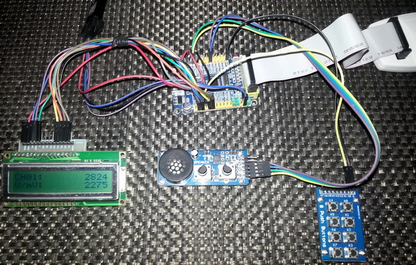
External Interrupt Triggered Single Channel Single Conversion Mode
Up till now the ADC trigger was given from the software end. However STM32 micros can perform ADC conversions when triggered externally by some other hardware. In this example, an external interrupt pin is used to trigger a single ADC conversion. After completing an ADC conversion the ADC halts. We can also use timer events as trigger sources too.
#include "ADC.h"
#include "GPIO.h"
#include "AFIO.h"
#include "Ex_Int.h"
sbit LCD_RS at GPIOB_ODR.B1;
sbit LCD_EN at GPIOB_ODR.B2;
sbit LCD_D4 at GPIOB_ODR.B12;
sbit LCD_D5 at GPIOB_ODR.B13;
sbit LCD_D6 at GPIOB_ODR.B14;
sbit LCD_D7 at GPIOB_ODR.B15;
register unsigned int adc_data = 0;
void setup();
void GPIO_init();
void ADC_init();
void interrupts_init();
void lcd_print(unsigned char x_pos, unsigned char y_pos, unsigned int value);
float map(float v, float x_min, float x_max, float y_min, float y_max);
void void EXTI11_ISR()
iv IVT_INT_EXTI15_10
ics ICS_AUTO
{
if(read_pending_reg(11) != 0)
{
bit_set(GPIOC_ODR, 13);
delay_ms(10);
bit_clr(GPIOC_ODR, 13);
pending_clr(11);
}
}
void void ADC1_ISR()
iv IVT_INT_ADC1_2
ics ICS_AUTO
{
adc_data = (ADC1_DR & 0x0FFF);
}
void main()
{
float v = 0;
setup();
while(1)
{
v = map(adc_data, 0, 4095, 0, 3300);
lcd_print(13, 1, adc_data);
lcd_print(13, 2, v);
};
}
void setup()
{
GPIO_init();
ADC_init();
LCD_Init();
interrupts_init();
LCD_Cmd(_LCD_CLEAR);
LCD_Cmd(_LCD_CURSOR_OFF);
lcd_out(1, 1, "CH01:");
lcd_out(2, 1, "V/mV:");
}
void GPIO_init()
{
enable_GPIOA(enable);
enable_GPIOB(enable);
enable_GPIOC(enable);
pin_configure_low(GPIOA_CRL, 1, (analog_input | input_mode));
pin_configure_high(GPIOC_CRH, 13, (GPIO_PP_output | output_mode_medium_speed));
pin_configure_high(GPIOB_CRH, 11, (digital_input | input_mode));
pull_up_enable(GPIOB_ODR, 11);
}
void ADC_init()
{
ADC1_Enable();
clr_ADC1_settings();
set_ADC_mode(independent_mode);
set_ADC1_data_alignment(right_alignment);
set_ADC1_scan_conversion_mode(disable);
set_ADC1_continuous_conversion_mode(disable);
set_ADC1_sample_time(sample_time_71_5_cycles, 1);
set_ADC1_external_trigger_regular_conversion_edge(EXTI_11_trigger);
set_ADC1_regular_number_of_conversions(1);
set_ADC1_regular_sequence(1, 1);
set_ADC1_regular_end_of_conversion_interrupt(enable);
ADC1_calibrate();
start_ADC1();
}
void interrupts_init()
{
AFIO_enable(enable);
falling_edge_selector(11);
set_EXTI8_11(11, PB_pin);
interrupt_mask(11);
NVIC_IntEnable(IVT_INT_EXTI15_10);
NVIC_IntEnable(IVT_INT_ADC1_2);
EnableInterrupts();
}
void lcd_print(unsigned char x_pos, unsigned char y_pos, unsigned int value)
{
unsigned char tmp = 0;
tmp = (value / 1000);
lcd_chr(y_pos, x_pos, (tmp + 48));
tmp = ((value / 100) % 10);
lcd_chr_cp((tmp + 48));
tmp = ((value / 10) % 10);
lcd_chr_cp((tmp + 48));
tmp = (value % 10);
lcd_chr_cp((tmp + 48));
}
float map(float v, float x_min, float x_max, float y_min, float y_max)
{
return (y_min + (((y_max - y_min)/(x_max - x_min)) * (v - x_min)));
}
![External Interrupt Triggered Single Channel Single Conversion Mode (2)]()
![External Interrupt Triggered Single Channel Single Conversion Mode (1)]() Demo video link: https://www.youtube.com/watch?v=dT5wkXKs42E.
Demo video link: https://www.youtube.com/watch?v=dT5wkXKs42E.
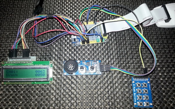
Single Injected Channel Continuous Conversion Mode
Previously I stated that injected groups are no different than regular groups when used alone. They will behave like regular groups if regular groups are absent. In this demo there’s no regular group channel and you’ll see that the injected group channel is behaving like a regular group channel.
#include "ADC.h"
#include "GPIO.h"
sbit LCD_RS at GPIOB_ODR.B1;
sbit LCD_EN at GPIOB_ODR.B2;
sbit LCD_D4 at GPIOB_ODR.B12;
sbit LCD_D5 at GPIOB_ODR.B13;
sbit LCD_D6 at GPIOB_ODR.B14;
sbit LCD_D7 at GPIOB_ODR.B15;
void setup();
void GPIO_init();
void ADC_init();
unsigned int read_ADC1();
void lcd_print(unsigned char x_pos, unsigned char y_pos, unsigned int value);
float map(float v, float x_min, float x_max, float y_min, float y_max);
void main()
{
register unsigned int adc_data = 0;
float V = 0.0;
setup();
while(1)
{
bit_set(GPIOC_ODR, 13);
delay_ms(10);
adc_data = read_ADC1();
V = map(adc_data, 0, 4095, 0, 3300);
lcd_print(13, 1, adc_data);
lcd_print(13, 2, V);
bit_clr(GPIOC_ODR, 13);
delay_ms(90);
};
}
void setup()
{
GPIO_init();
ADC_init();
LCD_Init();
LCD_Cmd(_LCD_CLEAR);
LCD_Cmd(_LCD_CURSOR_OFF);
lcd_out(1, 1, "CH03:");
lcd_out(2, 1, "V/mV:");
}
void GPIO_init()
{
enable_GPIOA(enable);
enable_GPIOB(enable);
enable_GPIOC(enable);
pin_configure_low(GPIOA_CRL, 3, (analog_input | input_mode));
pin_configure_high(GPIOC_CRH, 13, (GPIO_PP_output | output_mode_low_speed));
}
void ADC_init()
{
ADC1_Enable();
clr_ADC1_settings();
set_ADC_mode(independent_mode);
set_ADC1_data_alignment(right_alignment);
set_ADC1_scan_conversion_mode(disable);
set_ADC1_continuous_conversion_mode(enable);
set_ADC1_injected_number_of_conversions(1);
set_ADC1_sample_time(sample_time_239_5_cycles, 3);
set_ADC1_injected_sequence(4, 3);
set_ADC1_external_trigger_injected_conversion_edge(JSWSTART_trigger);
ADC1_calibrate();
start_ADC1();
}
unsigned int read_ADC1()
{
set_ADC1_injected_conversions(enable);
while(ADC1_SRbits.JEOC == 0);
return (ADC1_JDR1 & 0x0FFF);
}
void lcd_print(unsigned char x_pos, unsigned char y_pos, unsigned int value)
{
unsigned char tmp = 0;
tmp = (value / 1000);
lcd_chr(y_pos, x_pos, (tmp + 48));
tmp = ((value / 100) % 10);
lcd_chr_cp((tmp + 48));
tmp = ((value / 10) % 10);
lcd_chr_cp((tmp + 48));
tmp = (value % 10);
lcd_chr_cp((tmp + 48));
}
float map(float v, float x_min, float x_max, float y_min, float y_max)
{
return (y_min + (((y_max - y_min)/(x_max - x_min)) * (v - x_min)));
}
![Single Channel Continuous Conversion Mode (2)]()
![Single Channel Continuous Conversion Mode (1)]() Demo video link: https://www.youtube.com/watch?v=R1MuJaWrfn8.
Demo video link: https://www.youtube.com/watch?v=R1MuJaWrfn8.
Multiple Injected Channels in Discontinuous Conversion Mode
In discontinuous mode, each injected group channel is converted according to a sequence and after each channel conversion an injected channel end of conversion flag is set. Since there can be four channels in an injected group, their conversion results are stored in four separate data registers. We just need to read those data registers when valid data values are ready. To use discontinuous mode we must specify the number of channels in the discontinuous mode apart from how many channels that are actually present in the group.
#include "ADC.h"
#include "GPIO.h"
sbit LCD_RS at GPIOB_ODR.B1;
sbit LCD_EN at GPIOB_ODR.B2;
sbit LCD_D4 at GPIOB_ODR.B12;
sbit LCD_D5 at GPIOB_ODR.B13;
sbit LCD_D6 at GPIOB_ODR.B14;
sbit LCD_D7 at GPIOB_ODR.B15;
void setup();
void GPIO_init();
void ADC_init();
void read_ADC1_injected(unsigned int temp_data[3]);
void lcd_print(unsigned char x_pos, unsigned char y_pos, unsigned int value);
void main()
{
unsigned int channel_data[3];
setup();
while(1)
{
read_ADC1_injected(channel_data);
lcd_print(1, 2, channel_data[0]);
lcd_print(7, 2, channel_data[1]);
lcd_print(13, 2, channel_data[2]);
bit_set(GPIOC_ODR, 13);
delay_ms(10);
bit_clr(GPIOC_ODR, 13);
delay_ms(90);
};
}
void setup()
{
GPIO_init();
ADC_init();
LCD_Init();
LCD_Cmd(_LCD_CLEAR);
LCD_Cmd(_LCD_CURSOR_OFF);
lcd_out(1, 1, "CH00 CH01 CH02");
}
void GPIO_init()
{
enable_GPIOA(enable);
enable_GPIOB(enable);
enable_GPIOC(enable);
pin_configure_low(GPIOA_CRL, 0, (analog_input | input_mode));
pin_configure_low(GPIOA_CRL, 1, (analog_input | input_mode));
pin_configure_low(GPIOA_CRL, 2, (analog_input | input_mode));
pin_configure_high(GPIOC_CRH, 13, (GPIO_PP_output | output_mode_low_speed));
}
void ADC_init()
{
ADC1_Enable();
clr_ADC1_settings();
set_ADC_mode(independent_mode);
set_ADC1_data_alignment(right_alignment);
set_ADC1_scan_conversion_mode(disable);
set_ADC1_continuous_conversion_mode(disable);
set_ADC1_injected_number_of_conversions(3);
set_ADC1_sample_time(sample_time_28_5_cycles, 0);
set_ADC1_sample_time(sample_time_41_5_cycles, 1);
set_ADC1_sample_time(sample_time_13_5_cycles, 2);
set_ADC1_injected_sequence(1, 0);
set_ADC1_injected_sequence(2, 2);
set_ADC1_injected_sequence(3, 1);
set_ADC1_number_of_discontinuous_conversions(3);
set_ADC1_external_trigger_injected_conversion_edge(JSWSTART_trigger);
set_ADC1_discontinuous_conversion_mode_in_injected_mode(enable);
ADC1_calibrate();
start_ADC1();
}
void read_ADC1_injected(unsigned int temp_data[3])
{
set_ADC1_injected_conversions(enable);
while(ADC1_SRbits.JEOC == 0);
temp_data[0] = (ADC1_JDR3 & 0x0FFF);
set_ADC1_injected_conversions(enable);
while(ADC1_SRbits.JEOC == 0);
temp_data[1] = (ADC1_JDR2 & 0x0FFF);
set_ADC1_injected_conversions(enable);
while(ADC1_SRbits.JEOC == 0);
temp_data[2] = (ADC1_JDR1 & 0x0FFF);
}
void lcd_print(unsigned char x_pos, unsigned char y_pos, unsigned int value)
{
unsigned char tmp = 0;
tmp = (value / 1000);
lcd_chr(y_pos, x_pos, (tmp + 48));
tmp = ((value / 100) % 10);
lcd_chr_cp((tmp + 48));
tmp = ((value / 10) % 10);
lcd_chr_cp((tmp + 48));
tmp = (value % 10);
lcd_chr_cp((tmp + 48));
}
![Multiple Injected Channels in Discontinuous Conversion Mode (2)]()
![Multiple Injected Channels in Discontinuous Conversion Mode (1)]() Demo video link: https://www.youtube.com/watch?v=YwymJs8LlNU.
Demo video link: https://www.youtube.com/watch?v=YwymJs8LlNU.
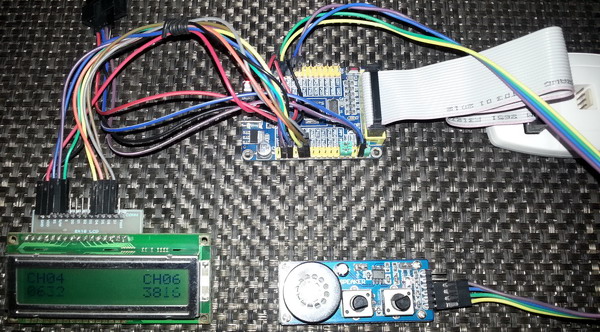
Multiple Injected Channels in Scan Conversion Mode
Scan mode is another interesting mode. In scan mode all ADC channels are scanned as per sequence. One conversion is performed for each channel. After having completed a scan an injected channel end of conversion flag is set. If interrupt is used then an end of conversion interrupt is issued. Scan mode is useful when we need to monitor several ADC channels, for example temperature and relative humidity. There’s a word of caution for using scan mode. STM32 reference manual states it like this:
Unlike a regular conversion sequence, if JL[1:0] length is less than four, the channels
are converted in a sequence starting from (4-JL). Example: ADC_JSQR[21:0] = 10
00011 00011 00111 00010 means that a scan conversion will convert the following
channel sequence: 7, 3, 3. (not 2, 7, 3)
This is why you’ll see some anomalies in this code example:
set_ADC2_injected_sequence(3, 4);
set_ADC2_injected_sequence(4, 6);
void ADC1_2_ISR()
iv IVT_INT_ADC1_2
ics ICS_AUTO
{
ADC2_SRbits.JEOC = 0;
channel_data[0] = (ADC2_JDR1 & 0x0FFF);
channel_data[1] = (ADC2_JDR2 & 0x0FFF);
}
Notice the sequence order and how the data is actually extracted. Keep this in mind while coding for injected groups in scan mode. Also note that in this code I used ADC2 instead of ADC1. This is not mandatory. I did so just to show that you can also use ADC2 rather than ADC1. For regular group channels the scan mode is DMA dependent because for regular group channels there’s only one data register for all the regular channels. I didn’t find a good way to avoid using the DMA unit. Of course using DMA is a much more clever approach. Since I won’t be discussing about DMA in this issue, I’m skipping this part for future.
#include "ADC.h"
#include "GPIO.h"
sbit LCD_RS at GPIOB_ODR.B1;
sbit LCD_EN at GPIOB_ODR.B2;
sbit LCD_D4 at GPIOB_ODR.B12;
sbit LCD_D5 at GPIOB_ODR.B13;
sbit LCD_D6 at GPIOB_ODR.B14;
sbit LCD_D7 at GPIOB_ODR.B15;
unsigned int channel_data[2];
void setup();
void GPIO_init();
void ADC_init();
void lcd_print(unsigned char x_pos, unsigned char y_pos, unsigned int value);
void ADC1_2_ISR()
iv IVT_INT_ADC1_2
ics ICS_AUTO
{
ADC2_SRbits.JEOC = 0;
channel_data[0] = (ADC2_JDR1 & 0x0FFF);
channel_data[1] = (ADC2_JDR2 & 0x0FFF);
}
void main()
{
setup();
while(1)
{
bit_set(GPIOC_ODR, 13);
set_ADC2_injected_conversions(enable);
delay_ms(10);
lcd_print(1, 2, channel_data[0]);
lcd_print(13, 2, channel_data[1]);
bit_clr(GPIOC_ODR, 13);
delay_ms(90);
};
}
void setup()
{
GPIO_init();
LCD_Init();
ADC_init();
LCD_Cmd(_LCD_CLEAR);
LCD_Cmd(_LCD_CURSOR_OFF);
lcd_out(1, 1, "CH04 CH06");
}
void GPIO_init()
{
enable_GPIOA(enable);
enable_GPIOB(enable);
enable_GPIOC(enable);
pin_configure_low(GPIOA_CRL, 4, (analog_input | input_mode));
pin_configure_low(GPIOA_CRL, 6, (analog_input | input_mode));
pin_configure_high(GPIOC_CRH, 13, (GPIO_PP_output | output_mode_low_speed));
}
void ADC_init()
{
ADC2_Enable();
clr_ADC2_settings();
set_ADC_mode(independent_mode);
set_ADC2_data_alignment(right_alignment);
set_ADC2_scan_conversion_mode(enable);
set_ADC2_continuous_conversion_mode(disable);
set_ADC2_sample_time(sample_time_1_5_cycles, 4);
set_ADC2_sample_time(sample_time_13_5_cycles, 6);
set_ADC2_external_trigger_injected_conversion_edge(JSWSTART_trigger);
set_ADC2_injected_number_of_conversions(2);
set_ADC2_injected_sequence(3, 4);
set_ADC2_injected_sequence(4, 6);
set_ADC2_injected_end_of_conversion_interrupt(enable);
NVIC_IntEnable(IVT_INT_ADC1_2);
EnableInterrupts();
ADC2_calibrate();
start_ADC2();
}
void lcd_print(unsigned char x_pos, unsigned char y_pos, unsigned int value)
{
unsigned char tmp = 0;
tmp = (value / 1000);
lcd_chr(y_pos, x_pos, (tmp + 48));
tmp = ((value / 100) % 10);
lcd_chr_cp((tmp + 48));
tmp = ((value / 10) % 10);
lcd_chr_cp((tmp + 48));
tmp = (value % 10);
lcd_chr_cp((tmp + 48));
}
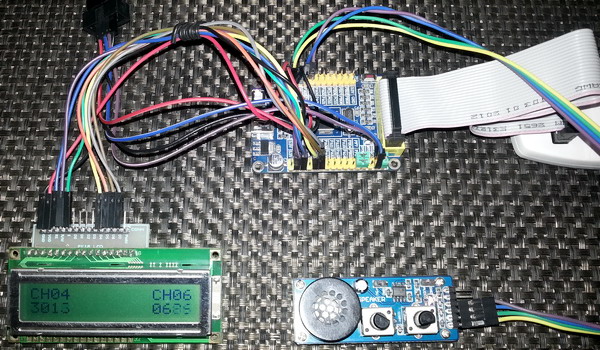
![Multiple Injected Channels in Scan Conversion Mode (2)]()
![Multiple Injected Channels in Scan Conversion Mode (1)]() Demo video link: https://www.youtube.com/watch?v=Mjax8dwClGE.
Demo video link: https://www.youtube.com/watch?v=Mjax8dwClGE.
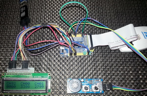
Regular Group Channels Discontinuous in Mode
This example is similar to the one I coded for injected group channels. It is somewhat an alternative of scan mode for regular group though technically they are not same. You can use this mode to monitor several ADC channels in a systematic order.
#include "ADC.h"
#include "GPIO.h"
sbit LCD_RS at GPIOB_ODR.B1;
sbit LCD_EN at GPIOB_ODR.B2;
sbit LCD_D4 at GPIOB_ODR.B12;
sbit LCD_D5 at GPIOB_ODR.B13;
sbit LCD_D6 at GPIOB_ODR.B14;
sbit LCD_D7 at GPIOB_ODR.B15;
unsigned char channel_no = 0;
unsigned int ch_data[3] = {0x0000, 0x0000, 0x0000};
void setup();
void GPIO_init();
void ADC_init();
void lcd_print(unsigned char x_pos, unsigned char y_pos, unsigned int value);
void ADC1_2_ISR()
iv IVT_INT_ADC1_2
ics ICS_AUTO
{
ADC2_SRbits.EOC = 0;
ch_data[channel_no] = (ADC2_DR & 0x0FFF);
channel_no++;
}
void main()
{
unsigned char s = 0;
setup();
while(1)
{
bit_set(GPIOC_ODR, 13);
set_ADC2_regular_conversions(enable);
while(channel_no < 3);
channel_no = 0;
for(s = 0 ; s < 3; s++)
{
lcd_print(((s * 6) + 1), 2, ch_data[s]);
}
bit_clr(GPIOC_ODR, 13);
};
}
void setup()
{
GPIO_init();
ADC_init();
LCD_Init();
LCD_Cmd(_LCD_CLEAR);
LCD_Cmd(_LCD_CURSOR_OFF);
lcd_out(1, 1, "CH02 CH00 CH01");
}
void GPIO_init()
{
enable_GPIOA(enable);
enable_GPIOB(enable);
enable_GPIOC(enable);
pin_configure_low(GPIOA_CRL, 0, (analog_input | input_mode));
pin_configure_low(GPIOA_CRL, 1, (analog_input | input_mode));
pin_configure_low(GPIOA_CRL, 2, (analog_input | input_mode));
pin_configure_high(GPIOC_CRH, 13, (GPIO_PP_output | output_mode_low_speed));
}
void ADC_init()
{
ADC2_Enable();
clr_ADC2_settings();
set_ADC_mode(independent_mode);
set_ADC2_data_alignment(right_alignment);
set_ADC2_scan_conversion_mode(disable);
set_ADC2_continuous_conversion_mode(disable);
set_ADC2_regular_number_of_conversions(3);
set_ADC2_number_of_discontinuous_conversions(3);
set_ADC2_sample_time(sample_time_41_5_cycles, 0);
set_ADC2_sample_time(sample_time_13_5_cycles, 1);
set_ADC2_sample_time(sample_time_28_5_cycles, 2);
set_ADC2_regular_sequence(1, 0);
set_ADC2_regular_sequence(2, 1);
set_ADC2_regular_sequence(3, 2);
set_ADC2_external_trigger_regular_conversion_edge(SWSTART_trigger);
set_ADC2_discontinuous_conversion_mode_in_regular_mode(enable);
set_ADC2_regular_end_of_conversion_interrupt(enable);
NVIC_IntEnable(IVT_INT_ADC1_2);
EnableInterrupts();
ADC2_calibrate();
start_ADC2();
}
void lcd_print(unsigned char x_pos, unsigned char y_pos, unsigned int value)
{
unsigned char tmp = 0;
tmp = (value / 1000);
lcd_chr(y_pos, x_pos, (tmp + 48));
tmp = ((value / 100) % 10);
lcd_chr_cp((tmp + 48));
tmp = ((value / 10) % 10);
lcd_chr_cp((tmp + 48));
tmp = (value % 10);
lcd_chr_cp((tmp + 48));
}
![Regular Group Channels Discontinuous in Mode (1)]()
![Regular Group Channels Discontinuous in Mode (2)]() Demo video link: https://www.youtube.com/watch?v=pz-y_W2Lxr8.
Demo video link: https://www.youtube.com/watch?v=pz-y_W2Lxr8.
Dual Conversion Mode
One of the cool feature of STM32’s ADC is its ability to simultaneous convert two ADC channels. This ability is sometimes highly demanded in some applications. For example in an energy meter you’ll need to measure both voltage and current simultaneous if you want precision. Applications like such demand the use of dual ADC mode. Please note that this feature is available only in those STM32 micros that have at least two ADC units. Fortunately there are only a few STM32 micros that have only one ADC unit. ST provided several sub modes for dual ADC modes but none attracted me much because those seemed to my achievable using one ADC and some programming tricks. It’s just my instinct. I could be wrong. To use dual ADC mode, we need to configure two ADC units separately. They’ll have some common setups. The individual ADCs are configured as such that as if they are configured for single ADC operation. The common settings are just ADC mode of operation setting and interrupt configuration. The results of ADC conversions of both channels are stored in ADC1_DR register Please note that ST recommends that we set the DMA bit for ADC1 even if we don’t use the DMA block itself.
#include "ADC.h"
#include "GPIO.h"
sbit LCD_RS at GPIOB_ODR.B1;
sbit LCD_EN at GPIOB_ODR.B2;
sbit LCD_D4 at GPIOB_ODR.B12;
sbit LCD_D5 at GPIOB_ODR.B13;
sbit LCD_D6 at GPIOB_ODR.B14;
sbit LCD_D7 at GPIOB_ODR.B15;
register unsigned long adc_data = 0;
void setup();
void GPIO_init();
void ADC_init();
void setup_ADC1();
void setup_ADC2();
void setup_common_ADC_settings();
void lcd_print(unsigned char x_pos, unsigned char y_pos, unsigned int value);
void ADC1_2_ISR()
iv IVT_INT_ADC1_2
ics ICS_AUTO
{
ADC1_SRbits.EOC = 0;
ADC2_SRbits.EOC = 0;
adc_data = adc1_dr;
bit_set(GPIOC_ODR, 13);
}
void main()
{
unsigned int adc1_data = 0;
unsigned int adc2_data = 0;
setup();
while(1)
{
set_ADC1_regular_conversions(enable);
adc1_data = (adc_data & 0x00000FFF);
adc2_data = ((adc_data & 0x0FFF0000) >> 16);
lcd_print(1, 2, adc1_data);
lcd_print(13, 2, adc2_data);
bit_clr(GPIOC_ODR, 13);
delay_ms(90);
};
}
void setup()
{
GPIO_init();
ADC_init();
LCD_Init();
LCD_Cmd(_LCD_CLEAR);
LCD_Cmd(_LCD_CURSOR_OFF);
lcd_out(1, 1, "CH00 CH01");
}
void GPIO_init()
{
enable_GPIOA(enable);
enable_GPIOB(enable);
enable_GPIOC(enable);
pin_configure_low(GPIOA_CRL, 0, (analog_input | input_mode));
pin_configure_low(GPIOA_CRL, 1, (analog_input | input_mode));
pin_configure_high(GPIOC_CRH, 13, (GPIO_PP_output | output_mode_low_speed));
}
void ADC_init()
{
setup_ADC1();
setup_ADC2();
setup_common_ADC_settings();
}
void setup_ADC1()
{
ADC1_Enable();
clr_ADC1_settings();
set_ADC1_data_alignment(right_alignment);
set_ADC1_scan_conversion_mode(disable);
set_ADC1_continuous_conversion_mode(disable);
set_ADC1_sample_time(sample_time_41_5_cycles, 0);
set_ADC1_external_trigger_regular_conversion_edge(SWSTART_trigger);
set_ADC1_regular_number_of_conversions(1);
set_ADC1_regular_sequence(1, 0);
set_ADC1_regular_end_of_conversion_interrupt(enable);
ADC1_calibrate();
start_ADC1();
}
void setup_ADC2()
{
ADC2_Enable();
clr_ADC2_settings();
set_ADC2_data_alignment(right_alignment);
set_ADC2_scan_conversion_mode(disable);
set_ADC2_continuous_conversion_mode(disable);
set_ADC2_sample_time(sample_time_41_5_cycles, 1);
set_ADC2_external_trigger_regular_conversion_edge(SWSTART_trigger);
set_ADC2_regular_number_of_conversions(1);
set_ADC2_regular_sequence(1, 1);
set_ADC2_regular_end_of_conversion_interrupt(enable);
ADC2_calibrate();
start_ADC2();
}
void setup_common_ADC_settings()
{
set_ADC1_DMA(enable);
set_ADC_mode(regular_simultaneous_mode_only);
NVIC_IntEnable(IVT_INT_ADC1_2);
EnableInterrupts();
}
void lcd_print(unsigned char x_pos, unsigned char y_pos, unsigned int value)
{
unsigned char tmp = 0;
tmp = (value / 1000);
lcd_chr(y_pos, x_pos, (tmp + 48));
tmp = ((value / 100) % 10);
lcd_chr_cp((tmp + 48));
tmp = ((value / 10) % 10);
lcd_chr_cp((tmp + 48));
tmp = (value % 10);
lcd_chr_cp((tmp + 48));
}
![Dual ADC Mode]() Demo video link: https://www.youtube.com/watch?v=sSGJUkX-mSg.
Demo video link: https://www.youtube.com/watch?v=sSGJUkX-mSg.
Injected Group vs. Regular Group
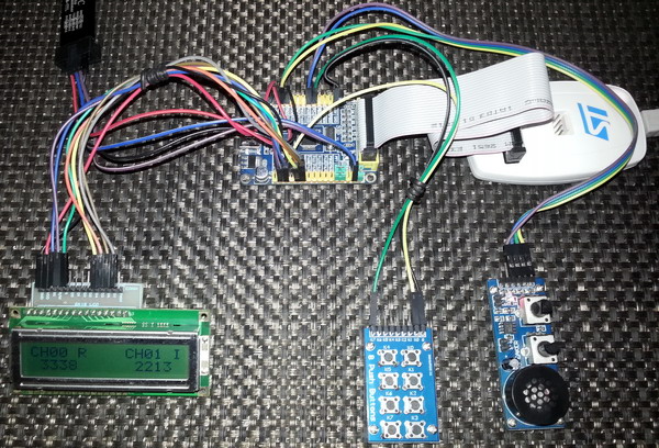
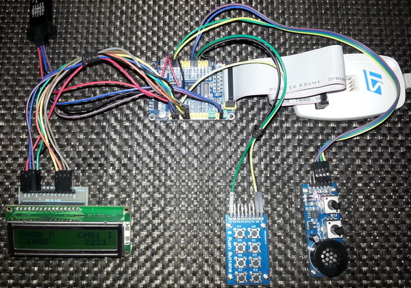
Till now we saw regular and injected groups independently. In this example we’ll see them together. There are two ADC channels. One of them belongs to regular group while the other belongs to injected group. We’ll see that the injected channel will override the conversion of regular channel. Both of these groups are triggered externally. A flashing LED is indicated which conversion is going on. Please check the video for better understanding.
#include "ADC.h"
#include "GPIO.h"
#include "AFIO.h"
#include "Ex_Int.h"
sbit LCD_RS at GPIOB_ODR.B1;
sbit LCD_EN at GPIOB_ODR.B2;
sbit LCD_D4 at GPIOB_ODR.B12;
sbit LCD_D5 at GPIOB_ODR.B13;
sbit LCD_D6 at GPIOB_ODR.B14;
sbit LCD_D7 at GPIOB_ODR.B15;
register unsigned int regular_adc_data = 0;
register unsigned int injected_adc_data = 0;
void setup();
void GPIO_init();
void ADC_init();
void exeternal_interrupt_init();
void lcd_print(unsigned char x_pos, unsigned char y_pos, unsigned int value);
void ADC1_2_ISR()
iv IVT_INT_ADC1_2
ics ICS_AUTO
{
if(ADC1_SRbits.EOC)
{
ADC1_SRbits.EOC = 0;
regular_adc_data = (ADC1_DR & 0x0FFF);
}
if(ADC1_SRbits.JEOC)
{
ADC1_SRbits.JEOC = 0;
injected_adc_data = (ADC1_JDR1 & 0x0FFF);
}
}
void void EXTI11_ISR()
iv IVT_INT_EXTI15_10
ics ICS_AUTO
{
unsigned char s = 0;
if(read_pending_reg(15) != 0)
{
for(s = 0; s < 3; s++)
{
bit_set(GPIOC_ODR, 13);
delay_ms(10);
bit_clr(GPIOC_ODR, 13);
delay_ms(10);
}
pending_clr(15);
}
if(read_pending_reg(11) != 0)
{
for(s = 0; s < 6; s++)
{
bit_set(GPIOC_ODR, 13);
delay_ms(90);
bit_clr(GPIOC_ODR, 13);
delay_ms(90);
}
pending_clr(11);
}
}
void main()
{
setup();
while(1)
{
lcd_print(2, 2, regular_adc_data);
lcd_print(12, 2, injected_adc_data);
};
}
void setup()
{
GPIO_init();
ADC_init();
exeternal_interrupt_init();
LCD_Init();
LCD_Cmd(_LCD_CLEAR);
LCD_Cmd(_LCD_CURSOR_OFF);
lcd_out(1, 1, "CH00 R");
lcd_out(1, 11, "CH01 I");
}
void GPIO_init()
{
enable_GPIOA(enable);
enable_GPIOB(enable);
enable_GPIOC(enable);
pin_configure_low(GPIOA_CRL, 0, (analog_input | input_mode));
pin_configure_low(GPIOA_CRL, 1, (analog_input | input_mode));
pin_configure_high(GPIOB_CRH, 11, (digital_input | input_mode));
pin_configure_high(GPIOC_CRH, 15, (digital_input | input_mode));
pin_configure_high(GPIOC_CRH, 13, (GPIO_PP_output | output_mode_low_speed));
pull_up_enable(GPIOB_ODR, 11);
pull_up_enable(GPIOC_ODR, 15);
}
void ADC_init()
{
ADC1_Enable();
clr_ADC1_settings();
set_ADC_mode(independent_mode);
set_ADC1_data_alignment(right_alignment);
set_ADC1_scan_conversion_mode(disable);
set_ADC1_continuous_conversion_mode(disable);
set_ADC1_sample_time(sample_time_239_5_cycles, 0);
set_ADC1_sample_time(sample_time_239_5_cycles, 1);
set_ADC1_injected_sequence(4, 1);
set_ADC1_injected_number_of_conversions(1);
set_ADC1_external_trigger_injected_conversion_edge(EXTI_15_trigger);
set_ADC1_injected_end_of_conversion_interrupt(enable);
set_ADC1_regular_sequence(1, 1);
set_ADC1_regular_number_of_conversions(1);
set_ADC1_external_trigger_regular_conversion_edge(EXTI_11_trigger);
set_ADC1_regular_end_of_conversion_interrupt(enable);
NVIC_IntEnable(IVT_INT_ADC1_2);
EnableInterrupts();
ADC1_calibrate();
start_ADC1();
}
void exeternal_interrupt_init()
{
AFIO_enable(enable);
falling_edge_selector(11);
falling_edge_selector(15);
set_EXTI8_11(11, PB_pin);
set_EXTI12_15(15, PC_pin);
interrupt_mask(11);
interrupt_mask(15);
NVIC_IntEnable(IVT_INT_EXTI15_10);
}
void lcd_print(unsigned char x_pos, unsigned char y_pos, unsigned int value)
{
unsigned char tmp = 0;
tmp = (value / 1000);
lcd_chr(y_pos, x_pos, (tmp + 48));
tmp = ((value / 100) % 10);
lcd_chr_cp((tmp + 48));
tmp = ((value / 10) % 10);
lcd_chr_cp((tmp + 48));
tmp = (value % 10);
lcd_chr_cp((tmp + 48));
}
![Injected vs Regular (1)]()
![Injected vs Regular (2)]() Demo video link: https://www.youtube.com/watch?v=K5XTYtVEoSo.
Demo video link: https://www.youtube.com/watch?v=K5XTYtVEoSo.
Common Pitfalls
When dealing with new stuffs, we often make some silly mistakes. In the case of STM32 ADC, the following mistakes are pretty much common:
- ADC not powered.
- ADC not calibrated.
- ADC settings not cleared/reset to defaults.
- Incorrect GPIO port selection and configuration. If a pin is to be set for an analogue input channel then it should be either kept floating or configured as analogue input.
- Wrong mode of operation selected.
- Incorrect peripheral clock selection.
- Same channels configured for different ADCs, for example CH0 configured for ADC1 and 2.
- Different sampling times for two simultaneous channels in dual conversion mode.
- Interrupts not enabled when using them. MikroC’s interrupt assistant feature should be used to avoid such mistakes. The interrupt assistant also help in code generation.
- Improper selection of regular and injected modes.
- Incorrect data alignment. Right alignment should always be used unless needed otherwise.
- Wrong variable type declaration. If the resulting data from a conversion is signed then signed integers should be used.
- Wrong ADC channel sequencing with incorrect channel order.
Final Words
There are many ways to meet a specific measurement case with STM32 ADCs. Imagination is the limit for so. As I stated earlier it is not possible for me to show all ADC operations in this post. Thus I would like readers to try and experiment whatever I showed. If you can take the challenge and if you have understood the basics then I would suggest that you experiment those stuffs which I didn’t cover. Finally there’s a saying
ADC + DMA = Unbeatable Assets
Of course the DMA block is an asset and when there’s an ADC-DMA collaboration, the result is a revolution in measurement. This issue was not regarding DMA and so when I cover the DMA block, I’ll show more about ADC. For now this post is enough to introduce the basics of STM32 ADC. Files: STM32 ADC Files. Happy coding.
Author: Shawon M. Shahryiar
https://www.facebook.com/groups/microarena
https://www.facebook.com/MicroArena
+8801970046495 18.03.2015