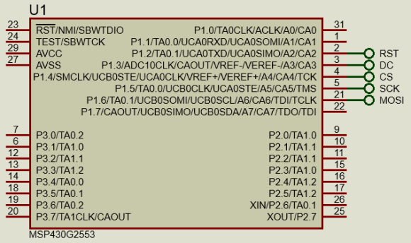
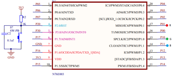
Texas Instruments (TI) is a well-known US-based semiconductor manufacturer. TI is perhaps best known to many as the manufacturer of some of the fanciest scientific calculators in the market. Of the long list of electronic devices produced by TI, microcontrollers are on the top. TI manufactures some of the coolest and advanced microcontrollers of the market today. There are several categories of micros from TI. These include general purpose low power MCUs which mainly comprise of MSP430s, ARMs like TM4Cs, MSP432s, etc, micros for wireless communications like CC2xxx series, ARM + DSP micros, DSP-specialized micros like the TMS32xxx series and so on. It will look as if TI is committed toward mixed signal microcontrollers that are engineered for highly sophisticated industrial challenges. This issue will cover an insight of value-line MSP430 general purpose micros.
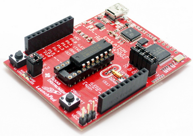
![MSP430 Launchpad Board]()
MSP430s are not seen as much as the popular 8051s, PICs and AVRs. In most of the Asian market, for example, MSP430s are rare when compared to other microcontrollers and even still rare when compared to other chips produced by TI itself. I don’t know why there is such an imbalance. Perhaps one big reason is its inclination towards low power consumption and limited resources. Low-power means that these MCUs are crafted for special low power applications unlike most other micros. Secondly TI micros are a bit expensive than other micros. Despites these, TI has provided some great tools for making things simple. You can get your hands on some cool MSP430 chips through some affordable Launchpad boards and still it worth every penny learning MSP430s. Firstly, it is a family of ultra-low power high performance 16-bit (16-bit data bus) micros which are unlike the popular 8-bit platforms. Secondly MSP430s have highly rich internal hardware peripherals that are second to none. For instance, MSP430s can be operated over a wide voltage and frequency ranges. Another great feature that is less common in most 8-bit micros is the DMA controller. Fortunately, MSP430s possess this. Probably it is your first such micro family that is somewhere between 8-bit and 32-bit micros. In the end, MSP430s will surely give you a taste of absolute American technology and concepts.
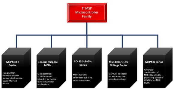
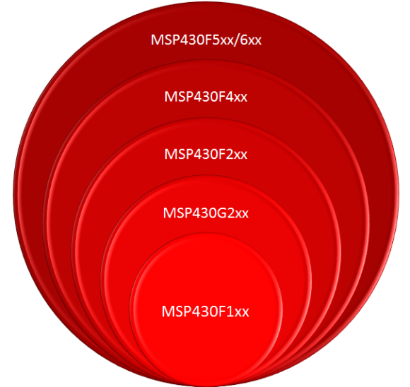
The MSP430 Family
Shown below is the family tree of MSP430 series microcontrollers from TI.
![TI MSP430 Family]()
The most common MSP430 micros are the MSP430FR series, MSP430F series, MSP430G series and the newly introduced MSP432 series.
MSP430FR series micros mainly feature high reliability, high endurance, 10-year data retention non-volatile FRAM (ferroelectric random-access memory) memories. This series offer 16-bit solutions for ultra-low-power sensing and system management in areas like smart building management systems, smart grids, military and industrial designs. They feature the lowest standby power consumption of about 350 nA with RTC, 100 µA/MHz active power consumption and the unique ability to save and instantly restore system state right after power failures.
MSP432 series micros are the perfect combinations of MSP430 low-power portfolio with advanced mixed-signal features and the high-performance processing capabilities of 32-bit ARM M4F engine. These micros have high measurement precisions and contain high performance peripherals like high resolution differential ADCs, DMA, IOT connectivity, etc. This series fills the gap between 16-bit MSP430s and 32-bit ARM architecture and as of this moment this series is the most recent development in the MSP430 family.
CC430 series is a small series of MSP430s with almost all features one can find in a typical MSP430 micro and embedded sub-GHz radio transceivers. They are well-stuffed true System-on-Chip (SOC) solutions that remove the necessity of additional off-board wireless solutions.
Yet another tiny series of MSP430 micros include MSP430Cxx and MSP430Lxx micros. These micros are intended for extreme low voltage (0.9 – 1.65V) operations. With just one Nickel Cadmium (NiCd) battery it is possible to run any micro of this series. They feature low resolution analogue frontends and low pin counts.
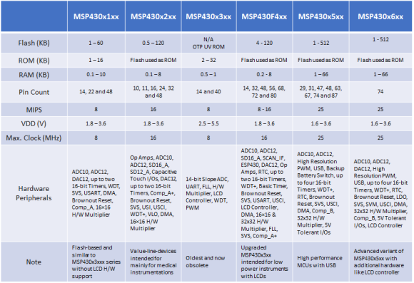
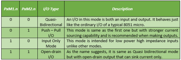
The only series that is left to be discussed is the general purpose MSP430s series microcontrollers. By general purpose, it is meant that these micros can be use in almost any scenario. It is this series of micros that we will be dealing here. The table below summarizes this family:
![General Purpose MSP430s]()
For now, don’t struggle to understand the abbreviations of this table. You’ll eventually know about them as we proceed.
![MSP430Fxxx and MSP430Gxxx]()
Note that there are some other MSP430 devices that are not accounted here. These devices are either rare or subset of the mentioned families. If you want to know more about MSP430 microcontrollers then you can go through the following Wikipedia article: https://en.wikipedia.org/wiki/TI_MSP430.
Launchpad Boards and BoosterPacks
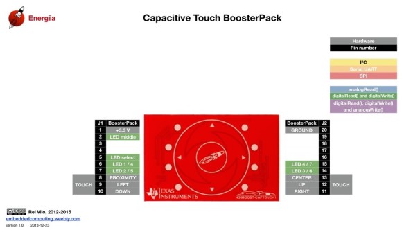
Launchpad boards are affordable MSP430 evaluation kits. For just few dollars, you can have your own Launchpad boards. They are so cheap that an average school-going student can afford one with his/her own pocket money. However, this cheapness doesn’t compromise quality nor performance. They are more-or-less alike Arduino boards in terms of board size and on-board resources except they don’t share same pin naming conventions and board layouts. Well that’s not a big issue. However, it would have been better if the Launchpads shared Arduino-like form factor. This would have enabled using Arduino shields with Launchpads. TI has, however, its own brand of shields called BoosterPacks and they seem to like promoting their own idea, owing to which there’s still no official TI Launchpad that share exactly Arduino form-factor/shape. It is a very aggressive marketing boldness. Shown below is the BOOSTXL-EDUMKII BoosterPack. It is just like Arduino Esplora with lots of on-board sensors and devices except for the MCU. It is good for game development and sensor applications. There are other useful BoosterPacks dedicated for capacitive touch, displays and so on.
![BoosterPack]()
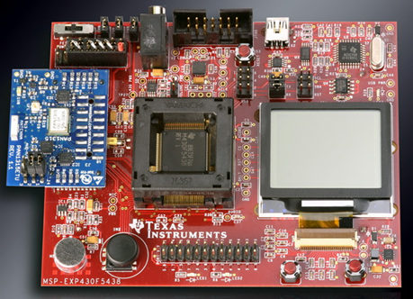
Launchpad boards are not the only development boards offered by TI. There are many other dev boards too. Shown below is the TI MSP-EXP430F5438 Bluetooth platform development board.
![MSP430 Bluetooth Development Platform]()
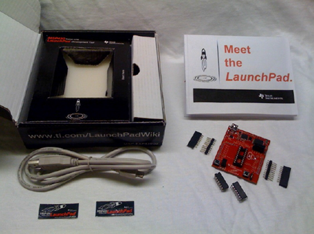
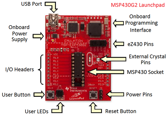
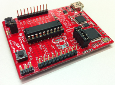
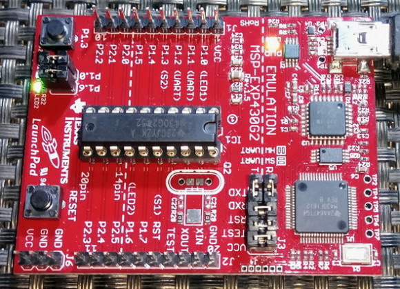
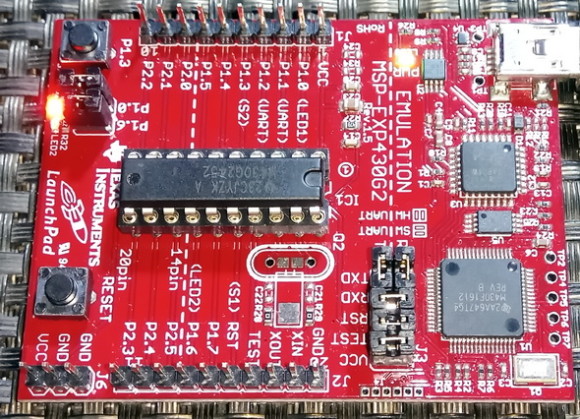
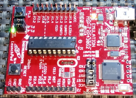
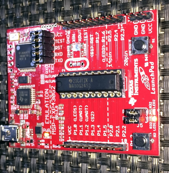
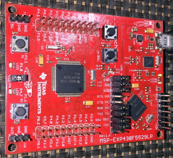
However due to cheapness and relatively good availability Launchpad boards are by far most popular, particularly the MSP-EXP430G2 Experimenter’s Launchpad board.
![Launchpad Box]()
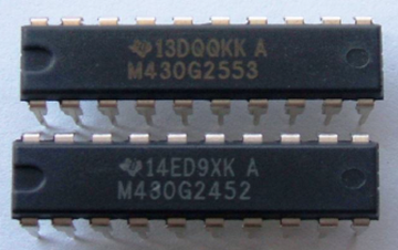
This board comes boxed with two micros – MSP430G2452 and MSP430G2553. Both of these mixed-signal MCUs come in PDIP packages. We can take them off from the board and use them in bread boards, strip boards, PCBs, etc. Shown below is the layout of a MSP-EXP430G2 Launchpad board.
![Launchpad Board Layout]()
Just like any other evaluation kit, every Launchpad comes embedded with user LEDs, buttons, I/O port headers (also known as BoosterPack connectors), onboard power supply, USB-to-serial converter and programming interfaces.
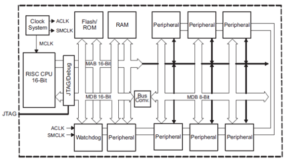
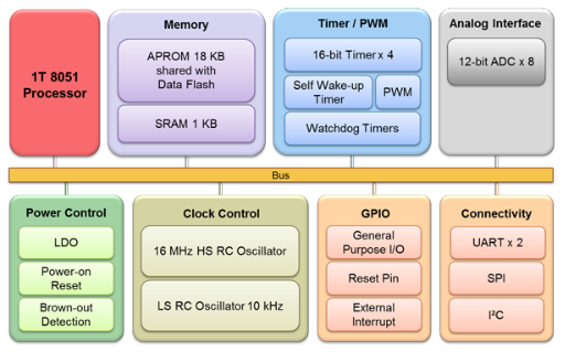
MSP430s are ultra-low power 16-bit general purpose microcontrollers. A MSP430 micro consists of a 16-bit RISC CPU, wide variety of feature-rich peripherals and a flexible clock system all under the hood of a von-Neumann architecture. Because of their ultra-low energy consumption profile, MSP430s are well-suited for battery/solar powered/limited or renewable energy applications.
![MSP430 Internal Architecture]()
MSP430G2452 and MSP430G2553 are both almost identical in terms of hardware peripherals and pin count. MSP430G2553 has some additional hardware features like more RAM-ROM memories, timers and USCI-based hardware interfaces for LIN and IrDA communications.
![MSP430 Value-Line Chips]()
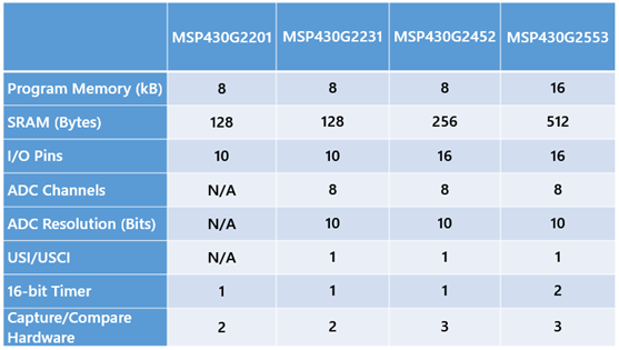
Shown below is a comparison table of some common MSP430 chips usually found with Launchpad boards.
![Comparison of Various MSP430 Value Line Devices]()
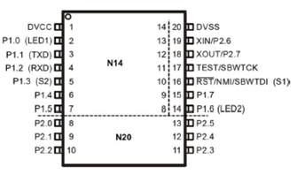
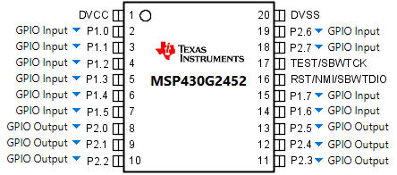
Other Launchpad boards contain other chips but fortunately they share the same pin layout and so they are fully pin compatible. The fourteen pin parts and twenty pin parts share the same pin layout as shown below:
![MSP430 Pin Compatibility]()
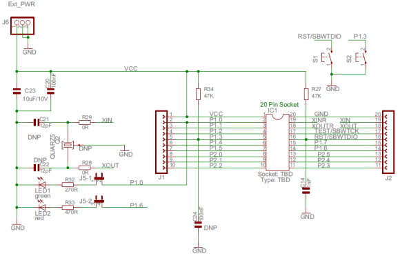
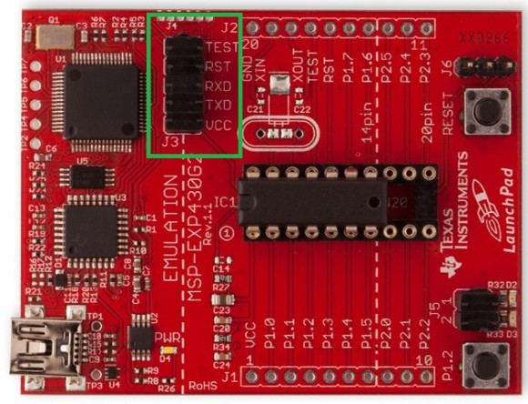
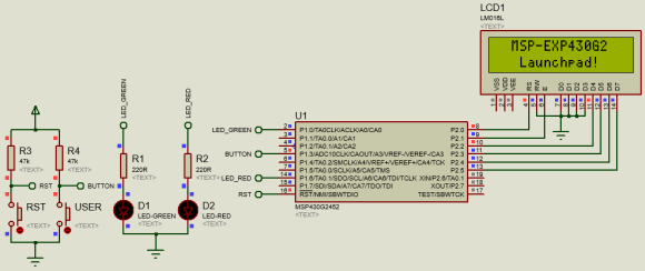
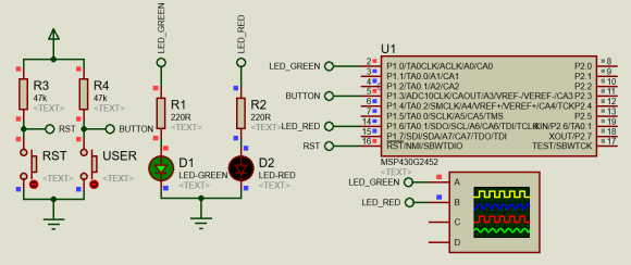
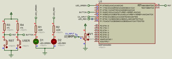
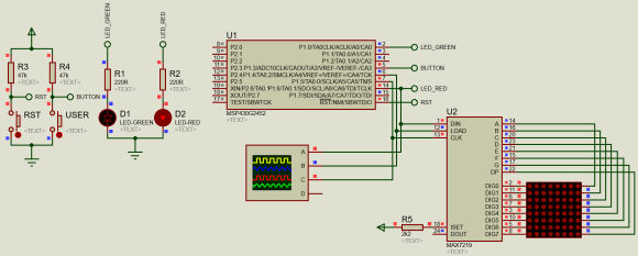
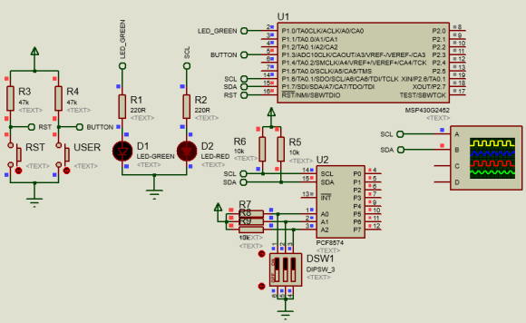
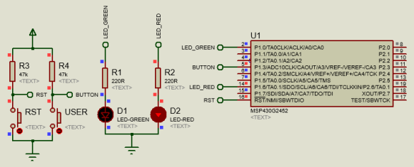
Though the pin names are labelled properly on the silkscreens of the boards, it is sometimes necessary to check the schematic for details. Shown below is the basic schematic of a MSP-EXP430G2 Launchpad.
![MSP430G2 Launchpad Basic Schematic]()
From the schematic, we can see what has been placed on the board by default. Parts labelled DNP are not placed on a fresh Launchpad board. These have been left for the users.
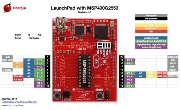
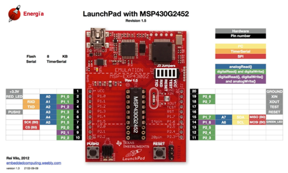
If these don’t matter much and you need something simpler, then there are Arduino-like pin maps for Launchpads. Though they are made for Energia IDE, they are useful for quick overviews.
![MSP430G2553 Pinmap]()
![MSP430G2452 Pinmap]()
Hardware
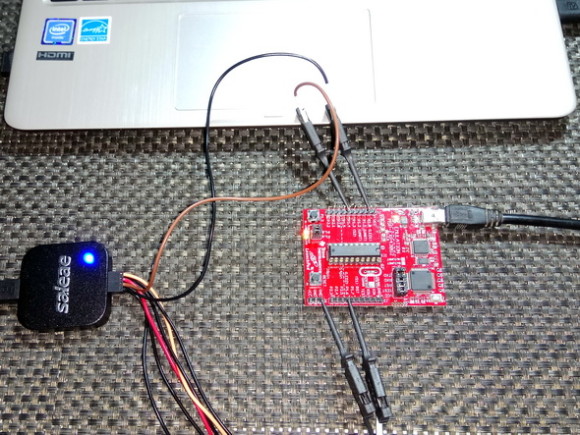
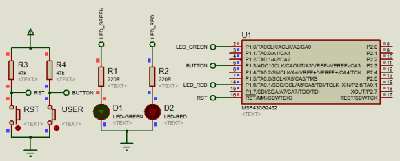
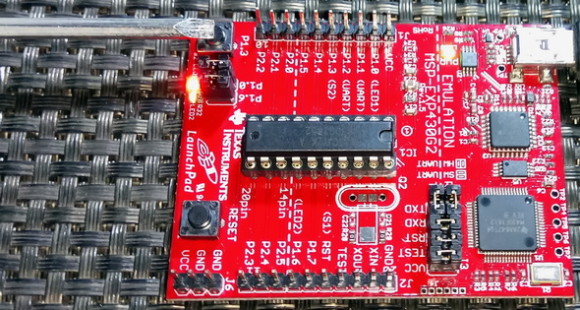
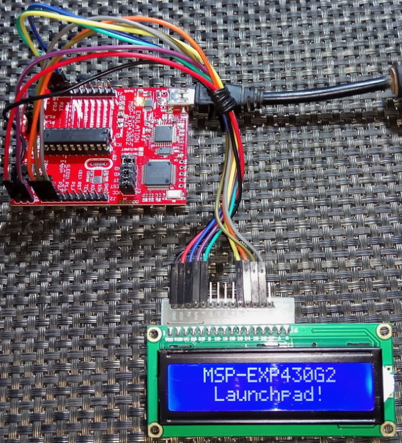
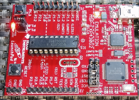
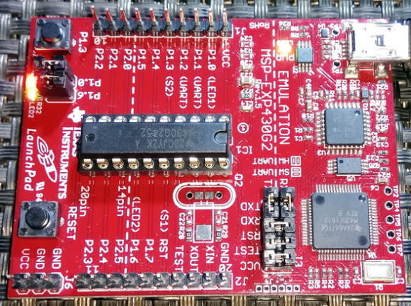
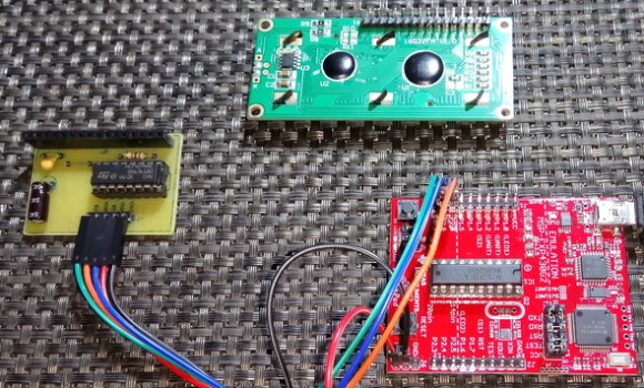
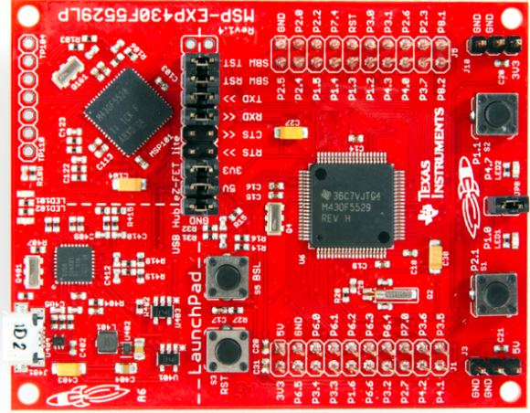
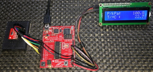
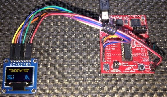
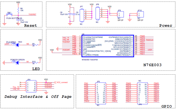
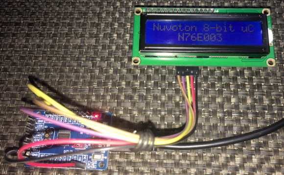
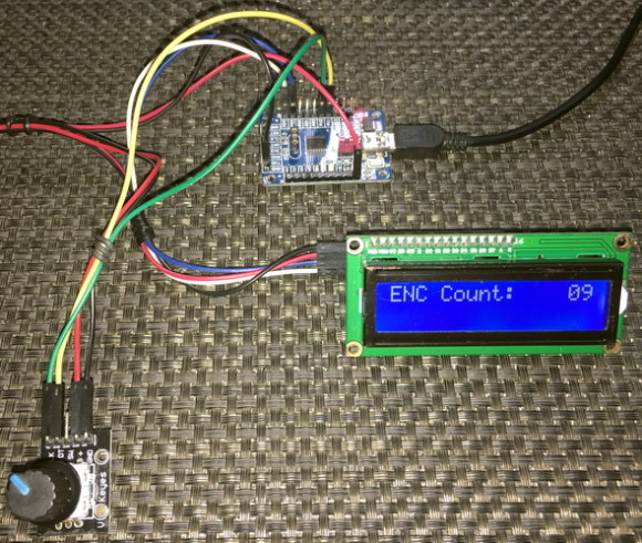
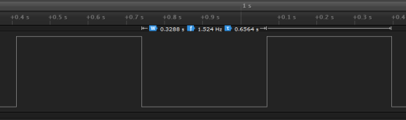
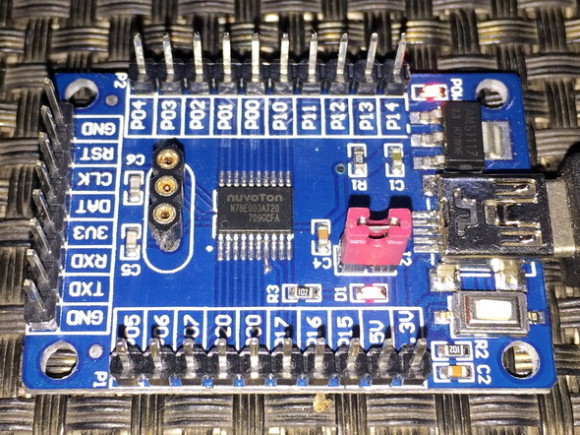
We will obviously need a MSP430 Launchpad board. For this tutorial, I used MSP-EXP430G2 Launchpad board with MSP430G2553 and MSP430G2452 microcontrollers.
![VLD Launchpad Board]()
Apart from the Launchpad board, we will need basic tools like a digital multimeter (DMM), wires or jumper cables, a power bank and other stuffs typically available in an Arduino starter kit like the RIASpire one shown below.
![RIAspire Arduino Starter Kit]()
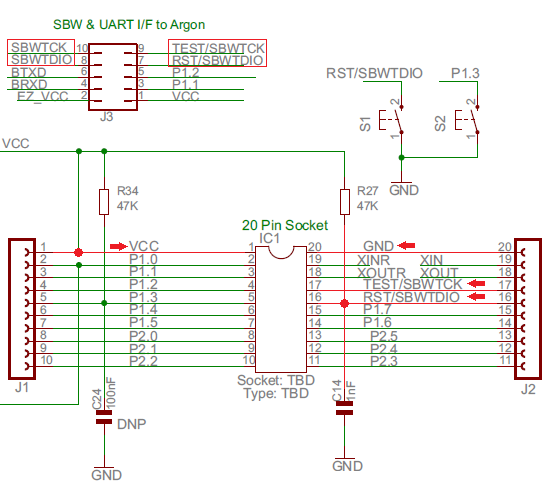
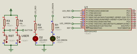
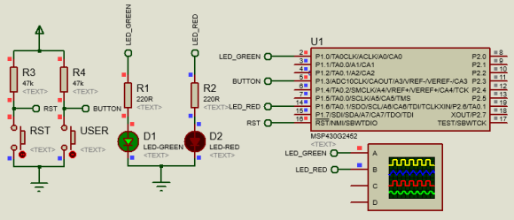
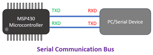
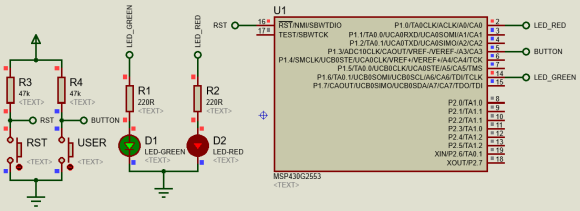
An additional external or off board programmer/debugger is not needed since MSP430 Launchpad boards come with on board Spy-Bi-Wire (SBW) programming/debugging interface. This interface utilizes pins labelled TEST and RST apart from power pins and so only four wires are needed. Note reset pin should be externally pulled up. Check the diagram below.
Similarly, we don’t need to buy/use any external USB-serial converter for serial communication as the boards come with onboard hardware for this communication.
![Spy-Bi-Wire Interface]()
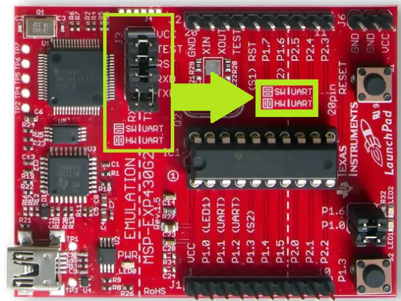
In all Launchpad boards, there are headers with jumpers as shown below to separate onboard programmer from the target. This allows us to use a Launchpad board as standalone programmer. We can also detach it. The top dotted line marks the border between the target and the programmer.
![SWI]()
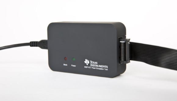
It is still nice to have one external MSP-FET programmer. FET stands for Flash Emulation Tool and it supports both JTAG and SWD interfaces. FETs are pretty expensive tools.
![MSP-FET Programmer]()
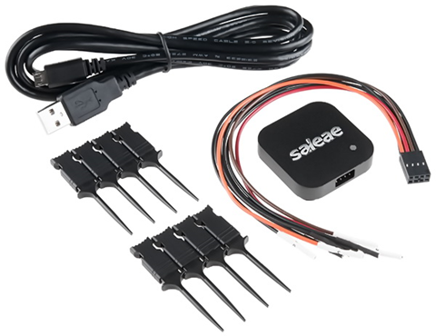
Lastly, I strongly recommend having an oscilloscope or a logic analyser for checking signals and timing-related info. In many cases, informations provided by these tools become extremely necessary.
![Logic Analyzer]()
![Analyzer and Oscilloscope]()
Software
There are numerous ways of learning and using a new microcontroller family effectively. A number of C/C++ compilers are available for coding MSP430 micros. Hobbyists and novice users find Arduino-like solutions easy and quick but from an engineer’s perspective such solutions are inexplicably incapable of extracting the sweet fruits of a well-armed microcontroller. Rawer approaches are preferred by professionals but they too seek reduced efforts and quick solutions. The learning curve is also needed to be a smooth one. In this segment, we will checkout some common software solutions for MSP430s.
Firstly, there is the free open-source Energia IDE. This is an Arduino-like IDE that enables users to code MSP430s in the Arduino way. It supports many Launchpad boards including those which are based on ARM cores. I have used it a lot and it is fun using it for simple hobby projects. However, I wanted to harness the true power of MSP430s. As with Arduino, you can access MSP430 registers in Energia too but that doesn’t make significant differences in terms of coding efficiency and memory consumptions. Energia has the same issues as with Arduino. Arduino framework on top of an AVR makes it much less robust when compared to a crude AVR. The same thing applies for Energia too. Another key limitation of Energia is the fact that not all MSP430 chips are supported by it. Energia is, however, very easy to use, quick and useful for rapid prototyping or testing. The costs are low overall efficiency and larger code size. Just like Arduino, Energia is not well-suited for highly sophisticate professional projects. It is just a rapid prototyping tool that we can use to check a proof-of-concept but not the right tool to build that concept. A smaller hammer is useful for nailing a pin but it is not the perfect tool for breaking a giant boulder.
Energia is available at http://energia.nu/.
![Energia IDE]()
Please note that Energia is not supported by the Arduino LCC which means it not developed or maintained by the guys from the Arduino team. This doesn’t matter much for its users. However, the IDE is not frequently updated like the Arduino IDE.
Next, we have TI’s own compiler – the Code Composer Studio (CCS). CCS is a C/C++ compiler based on Eclipse IDE. CCS comes with TI’s proprietary compilers that are best in code optimization. Those who have used Eclipse-based IDEs before know the advantages Eclipse framework brings with it. It has an excellent code navigation system, perspective views, refactoring, etc. CCS compiler comes with all of these stuffs and many more like debugger interface and TI App Store. Apart from all these there are some helpful cloud-based tools from TI. This tutorial is based on CCS compiler. It is free for download from TI’s website – http://www.ti.com/tool/ccstudio. Make sure you have a TI account.
![CCS IDE]()
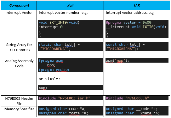
Then there is IAR compiler. I have never used IAR products but I have heard from many that it is very popular and widely used. However, it is expensive too.
Lastly, like for many other platforms we have the free open-source GCC compiler for MSP430s. MSP430 GCC can be integrated with CCS IDE.
We will see during coding that compilers don’t make significant differences in coding style, making codes cross-platform compatible. I also intend to keep things simple and quick. This is why I focus on tools rather than other stuffs. With right set of tools, any issue can be addressed decently and rapidly.
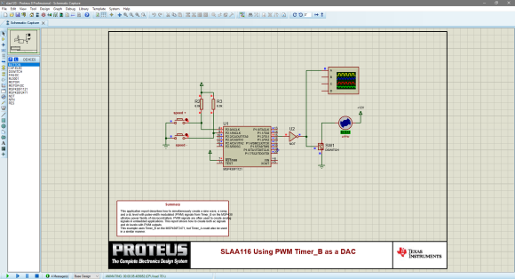
Additionally, some more software tools are needed for supportive purposes. Proteus VSM is a good interactive simulator cum PCB design software. Luckily it supports MSP430 micros. However, it is very expensive unless you are using a pirated version of it. Frankly speaking, I have never advocated for simulations because simulations do not address the real-world challenges we encounter in a real-life real-time project. Simulations, for example, cannot simulate real-world environment conditions nor can they emulate situations which result in “hang”-like stuck up conditions. Simulations don’t take the effect of noise and electromagnetic disturbances into account. Additionally, sometimes simulations give wrong results. I have spent many wasted hours trying to debug an issue with simulation only to find out that the simulation was incorrect. Still however, simulations are helpful in some special cases. For instance, when designing a LCD menu, simulation is a time and effort saver. Personally, I recommend and use real-world debugging over simulations. This gives me a lot of confidence.
![Proteus VSM]()
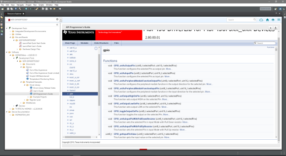
The coolest stuffs for MSP430s are TI’s MSP430Ware driver libraries (driverlib) and GRACE. Driver libraries remove the pain of traditionally coding MSP430s using registers. Driver libraries provide easy-to-use API functions for configuring MSP430 peripherals just like the Standard Peripheral Libraries (SPL) of STM8 micros. However, these libraries are only supported for the newest and resource-rich MSP430 microcontrollers like the MSP430F5529LP. This idea of driver libraries is quickly gaining mass popularity and is becoming standard day-by-day for all modern era micros. MSP430Ware can be downloaded for free from http://www.ti.com/tool/mspware.
![MSP430Ware]()
You can use TI’s Resource Explorer to check out what’s in driverlib and if your target MCU is supported.
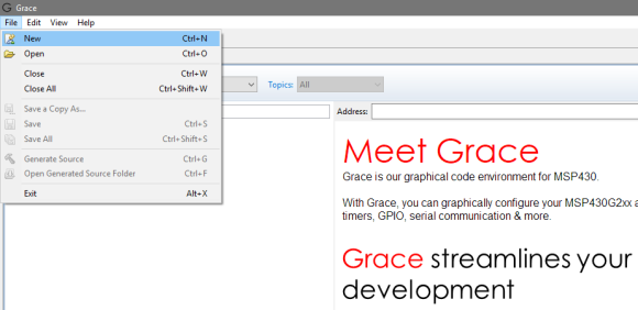
GRACE, on the other hand, is intended for relatively less-resourceful micros like the MSP430G2231 that are mostly well-suited for lower level assembly language environments. GRACE is basically a graphical code generator tool, much like the STM32CubeMX that can be used to generate setup configuration codes for MSP430F2xx, MSP430G2xx and some FR series micros. However, GRACE only generates register values for small MSP430 micros. For large and advanced MSP430 micros driverlib-based codes are generated instead of register-level codes. The rest is just like coding any other microcontroller. Throughout this tutorial, GRACE has been used for all demos.
![Grace]()
![Configuring BCS+ with Grace]()
![Grace Generated Code]()
As we can see the generated code snippet sets appropriate registers as per our setup in GRACE GUI.
GRACE can be downloaded without any charge from TI’s website: http://www.ti.com/tool/GRACE?keyMatch=grace%203&tisearch=Search-EN-Products.
We will also need a separate standalone programmer GUI tool. Why? Because it looks totally stupid to open the heavy CCS software every time to upload a code to a new target after having built the final code for it. For this purpose, we will need UniFlash programmer GUI.
![UniFlash GUI]()
UniFlash can be downloaded from http://www.ti.com/tool/uniflash or can be accessed via TI cloud.
Additionally, I recommend using Sublime Text (https://www.sublimetext.com/3) or Notepad++ (https://notepad-plus-plus.org/download/v7.4.2.html) as a code viewer/editor.
![Sublime Text]()
Make sure you also downloaded Launchpad board drivers from here: http://www.ti.com/lit/sw/slac524/slac524.zip.
Documents, Pages and Forums
The following documents must be acquired:
- Reference Manual
MSP430x2xx reference manual covers the details of all the hardware available in this family of microcontrollers. Unlike other microcontrollers, datasheet of a MSP430 micro, only says about technical specs and characteristics. Reference manuals say about internal hardware, how to use them and about internal registers. This is the most important document of all.
http://www.ti.com/lit/ug/slau144j/slau144j.pdf
- Launchpad User Manual and Associated Files
Visit the following link for Launchpad board user manual and other docs:
http://www.ti.com/tool/msp-exp430g2. This document not just introduces the Launchpad board, it also contains schematics, layouts and other stuffs. Off all the stuffs in the user manual, Launchpad board’s schematic is the most valuable thing.
- App Notes.
Though not mandatory, having a collection of MSP430 application notes is a surplus. These show various ideas and design concepts. Visit TI’s website for these docs.
There are some important websites, online communities and forums that are very helpful. Some of the most popular ones are:
http://www.43oh.com/
http://forum.43oh.com/
https://e2e.ti.com/support/microcontrollers/msp430/
http://processors.wiki.ti.com/index.php/Main_Page
http://www.ti.com/lsds/ti/microcontrollers-16-bit-32-bit/msp/overview.page
http://www.ti.com/lsds/ti/tools-software/launchpads/overview/overview.page
Starting a New CCS Project
Beginning a new CCS project is not too complicated. Provided that CCS is installed in your PC, simply run it.
![CCS Icon]()
In just a few seconds, CCS’s logo splashes.
![CCS Logo]()
You’ll be asked for workspace location. Either select an existing workspace if you have one or create a new one.
![Workspace Selection]()
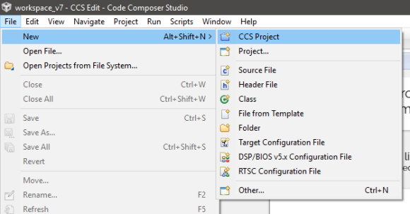
Next click File >> New >> CCS Project.
![CCS Project Selection]()
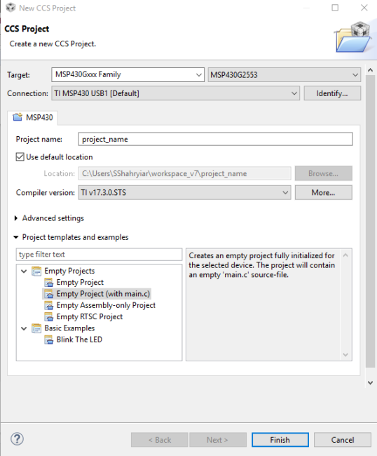
The following window will show up then:
![Project Parameter Setup]()
Here we just need to setup target MCU, name of the project, compiler version and project type. Keep other options unchanged unless you are sure of your actions.
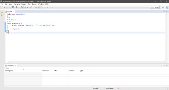
The following window appears after hitting the finish and we are good to go for coding. It is just that simple.
![Project Editor]()
One advice I would like to give here, never delete any workspace file or folder unless you created it. It is possible to rename and remove projects from CCS IDE.
GRACE
As stated earlier, GRACE is a graphical configuration tool. It reduces the effort of thoroughly reading datasheets and reference manuals. I highly recommend using it no matter if you are novice or expert.
First run GRACE.
![Grace Icon]()
Wait for it to launch.
![Grace Welcome Screen]()
TI’s Resource Explorer kicks in on first start up. It may not do so every time though.
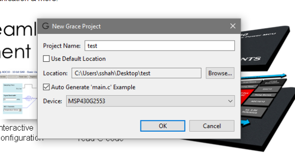
Click File >> New to begin a new GRACE project.
![New Grace Project]()
You’ll be prompted for project location, MCU part number and project name as shown below:
![Grace Project Properties]()
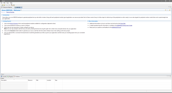
Once all the parameter fields are filled, we are ready to configure our target MCU. A welcome screen shows up next.
![Grace Project Overview]()
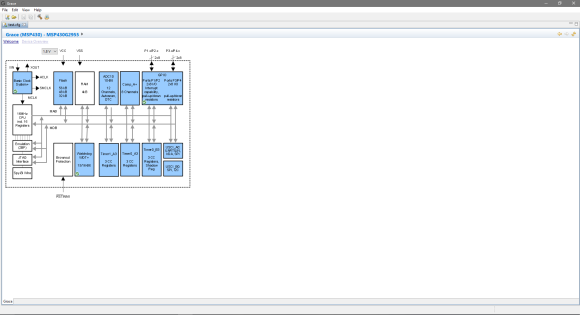
From the welcome screen, we have to click on Device Overview and get an insight of the device’s peripherals as peripheral blocks.
![Grace]()
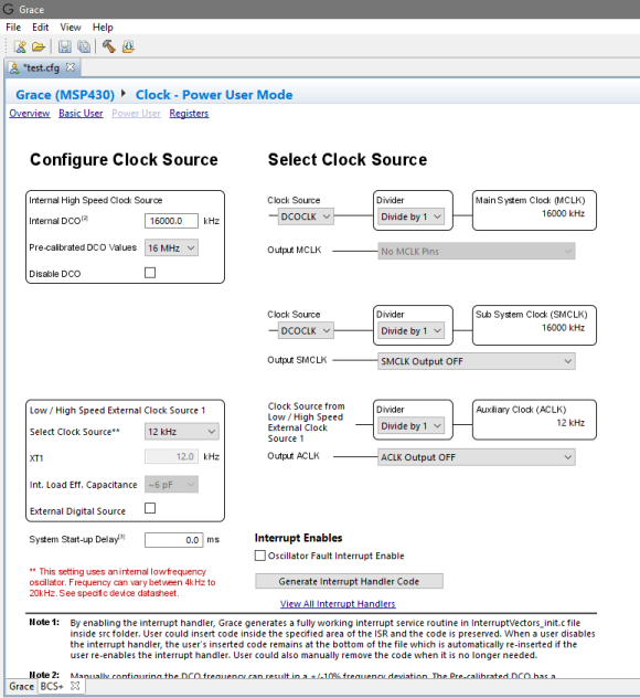
We can now click desired hardware peripheral block (blue blocks) to check what features and code examples it offers and set it up as required. There are two types of setups for all modules – Basic and Power users. Basic User setup is for simple setup when you don’t know everything of a peripheral in details and don’t want to mess things up. Power User setup is for expert users with more advanced options. Shown below are the Power User options for setting up the clock system:
![Configuring BCS+ with Grace]()
After setting up everything, just hit the hammer or Build button and the configuration codes are generated in the preset folder. It may take some time to complete the process. Next, we just need to open the generated files and copy them in our main CCS code.
How to create a new CCS project and use Grace is well documented in this video: https://www.youtube.com/watch?v=QCYMbsKwRfY.
UniFlash
Most of the times during development, a separate standalone programmer software is not a compulsory necessity as CCS IDE provides an inbuilt programmer/debugger interface. However, at times long after final application development, it becomes completely unnecessary to reopen CCS just to load a firmware to a new micro. UniFlash comes in aid at that time.
Run Uniflash by clicking its icon.
![UniFlash Icon]()
The following window appears:
![UniFlash GUI]()
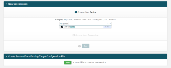
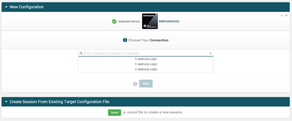
From here we need to select either target board or target microcontroller. No need to type the whole part number of a micro, just few digits/letters are enough to find the correct micro:
![UniFlash Chip Selection]()
Similarly, we need to setup connection to target too. USB1 – the first option is what we need to select.
![UniFlash Connection Selction]()
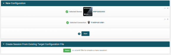
Now we are ready to begin firmware upload. Click the Start button.
![UniFlash Start Button]()
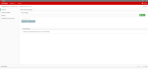
Browse the firmware you wish to upload.
![UniFlash File Selection]()
You can optionally set some more parameters for the target as shown:
![UniFlash Additional Properties]()
To flash new firmware, just hit the Load Image button.
Watch this video for details: https://www.youtube.com/watch?v=4uwQSSX-HrM.
Strategies and Tactics
Before we begin exploring MSP430 micros, I would like to discuss certain things though they may look like advanced stuffs for the moment.
Generating HEX Output Files
By default, CCS doesn’t generate any hex formatted output file. Everyone working in the embedded system sector is familiar with it. Hex outputs are useful for Proteus VSM simulations and loading code to a new MSP430 micro using an external programmer like UniFlash. Thus, it is essential if not imperative to unlock hex utility.
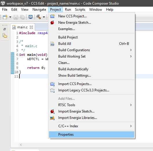
First go to Project >> Properties.
![Project Properties]()
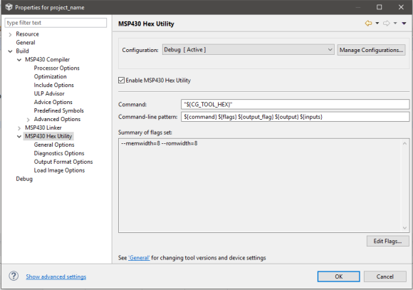
Navigate to find MSP430 Hex Utility and then enable it as shown below.
![Hex Utility]()
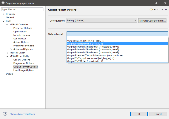
Finally select hex output format as shown:
![Hex File Format]()
Select Intel hex format as it is the one widely used.
Having set as shown, from now on, whenever you build your current project, you’ll get an output .hex file in the project’s debug/release folder depending on your project type selection.
Building New Libraries
Building new libraries is simple. All we need to do is to follow a few set of rules:
- For each module, there should be a separate header file and source file.
- Header file should contain definitions, variables, constants and function prototypes only.
- Header files should begin with the inclusion of MSP430 header file.
- Source files should include their respective header files and addition header files (if any).
- Source files should contain actual function codes only.
- Be aware of reserved keywords and constants.
- Global variables with same names should never be declared more than once.
- Empty functions and functions without prototypes must be avoided.
- Functions should have small and meaningful names.
- Be careful about case-senstivity, function type assignment and argument type of functions.
- Hierarchical order of library inclusion must be followed.
![Delay Library]()
Adding Custom Library Files
Adding own developed libraries to a project is key requirement for any software developer. This is because no compiler includes libraries for all hardware. We must realize a compiler as a tool only. The rest is how we use it and what we do with it. As for example, CCS comes with _delay_cycles instead of more commonly preferred delay_ms or delay_us functions. We will, thus, need software delay library. We need to code it and include it in our projects.
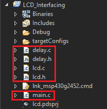
Custom libraries can be included in two ways. The easiest way is to add the include and source files in your projects root location, i.e. its folder. No additional job is needed because the root contains the main.c source file and its location is automatically included when you start a project.
![Root Library Location]()
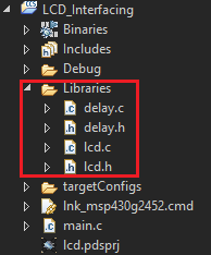
However, the aforementioned method becomes clumsy and unprofessional when there are too many custom library files in a large project and if you care for some neatness. The other method needs some additional tasks to be done before we can use our library files.
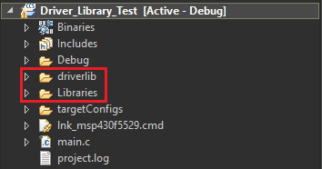
First make a folder in your project directory and give it a name. For example, I named this folder Libraries in my examples.
Next add the desired library source and header files in this folder.
![Library Folder]()
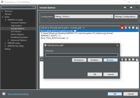
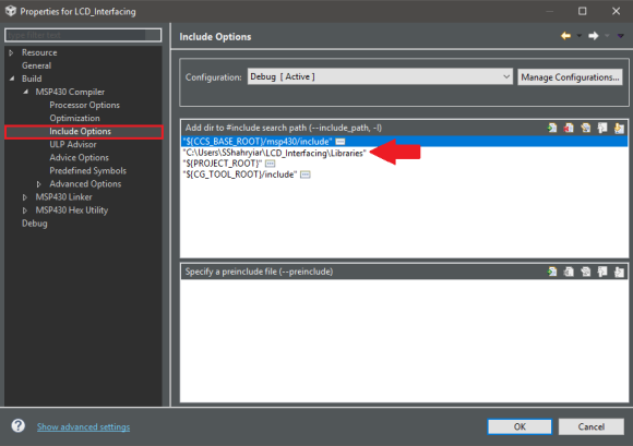
At this stage, we still cannot use these libraries because the compiler does not know their path(s) and so we need to inform the compiler about their location. We need to go to Project >> Properties first and then navigate to Include Options menu under Build >> MSP430 Compiler menu as shown:
![Library Folder Browse]()
Right after clicking the circled icon as shown above, we will be asked for folder location. It is just a simple browsing to the library folder location.
![Library Folder Inclusion]()
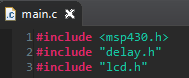
To use the libraries we added, we now just need to add some #include statements in our main.c file.
![Order of Include Files in Main Source Code]()
Be careful about the hierarchical order of library files because they may be interdependent. For example, as shown above, the LCD library has dependency on software delay library and so the delay library is added or called before the LCD library.
Using GRACE Simply but Effectively
GRACE should be used for quick setups. Who would like to waste time fixing register values when we have such a useful tool at our side. We will need a code viewer/editor like Sublime Text for viewing codes generated by GRACE. I like Sublime Text for its way of highlighting keywords and important stuffs with different colours. This helps in building quick situational awareness. A dark IDE is also good for night-time coding and less stressful for eyes.
Previously I showed how to use GRACE to generate configuration codes. GRACE generates individual source files for each hardware used. In this way, it doesn’t create too much mess. We will open each of these files with Sublime Text and copy only the needed init functions in our main source code. GRACE also generates other stuffs but that are like mere junks to us and so we will just ignore them.
![Important Parts in Grace]()
My code examples will give you an idea of what to copy. Keep in mind to stop the watchdog timer in the beginning of your code or it may reset your micro before entering actual application.
Optional Customizations
Explore the IDE Preferences for customizing CCS IDE according to your wishes. For instance, unlike the default white theme, I like a full black IDE interface like the one in Sublime Text. This is really effective when you work at night and in low light conditions. Just like Sublime Text key words are highlighted and it is easy to navigate in such an environment.
In a busy world, we often forget to update software in regular schedules and therefore miss important changes and bug fixes. Automatic updates come in aid in such case. I configured my CCS in such a way that it auto updates and notifies me about new software versions. I also added some tools from CCS/TI App Store like the GCC compiler.
Other customizations include MSP430Ware and EnergyTrace Technology debugger. EnergyTrace Technology allows us to compute energy consumptions. It helps in estimating battery requirements (if any).
I recommend readers to explore CCS IDE properties for more custom settings.
Advanced Concepts
Most of the times during code compilation you’ll notice that the compiler not only compiled your code but has also given you some optional advices. These advices aid in code optimizations and hint ways to enhance overall performance. For instance, it is better to use switch-case statements instead of if-else statements when dealing with fixed-discrete conditions. Try to follow the advices whenever possible. Same goes for compiler warnings. You must address the warnings for flawless coding.
In the internet, we can find lot of documents on C code optimization and good C language practices. Here is one such document from Atmel: http://www.atmel.com/images/doc8453.pdf. Although it was written for Atmel AVR microcontrollers but the document applies for all microcontrollers and C compilers. Similarly, Microchip has documents named Tips ‘n Tricks. Visit and search Microchip’s site for these documents These tricks and tips help in designs significantly. Try to follow these to achieve best utilization of your micro’s assets. TI’s application notes are also equally helpful literatures. Personally, I recommend studying the app notes, and other documents of other micro families too. This will help advance in developing new concepts, strategies and techniques.
Additionally, I would like to point out some issues and techniques when using CCS. Here are followings:
- Be careful about case sensitivity. Also, be careful about compiler’s reserved keywords and constants.
- Although not mandatory, it is, however, a good practice not to keep empty argument field in any function. Argumentless functions should have void argument instead of empty spaces.
- Flags are important event markers and so wherever they are present and needed you must use and check them unless automatically cleared. For instance, it necessary to clear timer flags upon exiting timer interrupts.
- Try to avoid polling methods. Try to use interrupt-based ones but make sure that there is no interrupt-within-interrupt case or otherwise your code may behave erratically. Best is to attach interrupts for important tasks like timing-related jobs, ADC conversions and communications. It is up to your design requirements and choices.
- Where fast processing is required, try to mix assembly with your C-code if you can or temporarily speed up your micro by increasing its oscillator speed or switching to a faster clock source. Checkout the assembly examples from TI’s Resource Explorer and MSP430Ware. Also try to study and learn about advanced C concepts like pointer, structures, functions, etc.
- Avoid empty loops and blank conditional statements.
- When you hover mouse cursor over a function, a small window appears. This window shows the internal coding of that function and relieve you from opening a new tab for it.
- CTRL + Space or code assist is a great helper. Likewise, CCS has some auto complete features.
- If you are using multiple computers during your project’s development stage, make sure that your custom library locations and workspace paths are properly added.
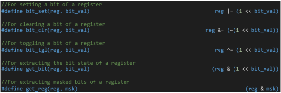
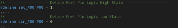
#define bit_set(reg, bit_val) reg |= (1 << bit_val) //For setting a bit of a register
#define bit_clr(reg, bit_val) reg &= (~(1 << bit_val)) //For clearing a bit of a register
#define bit_tgl(reg, bit_val) reg ^= (1 << bit_val) //For toggling a bit of a register
#define get_bit(reg, bit_val) (reg & (1 << bit_val)) //For extracting the bit state of a register
#define get_reg(reg, msk) (reg & msk) //For extracting masked bits of a register
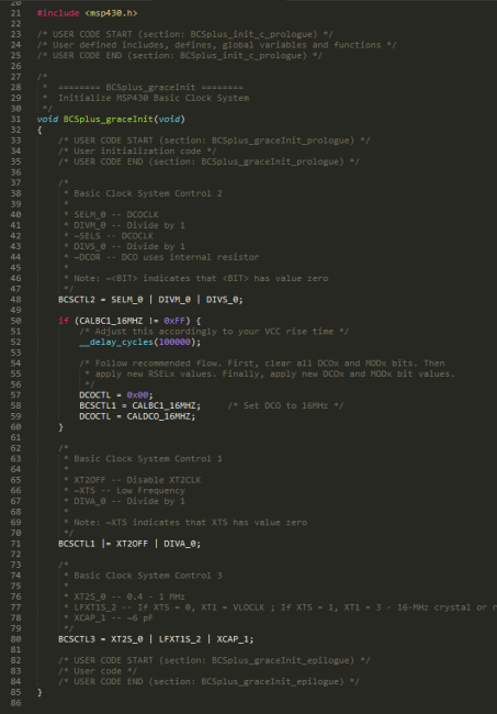
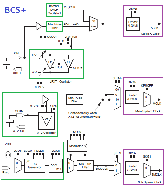
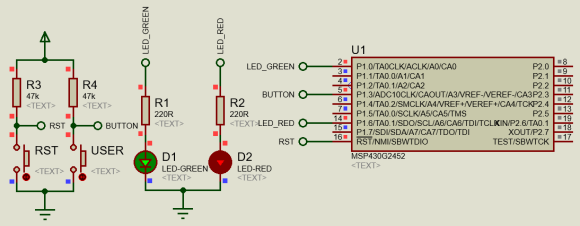
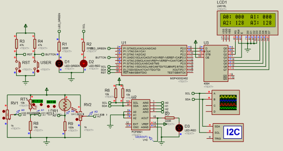
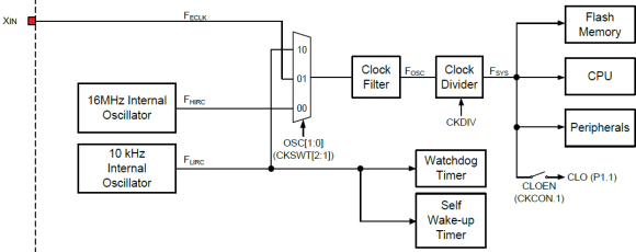
Basic Clock System Plus (BCS+)
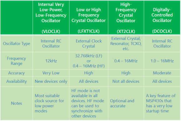
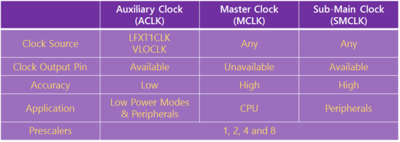
In all microcontrollers, power consumption and operating speed are interdependent and it is needed to balance these well to maximize overall performance while conserving energy. MSP430s are crafted with ultra-low power consumption feature in mind while not compromising performance. For this reason, MSP430s are equipped with a number of clock sources that vary in speed, accuracy and area of use. They also have clock dividers at various points apart from peripherals prescalers. This combination leads to a highly flexible clock system called Basic Clock System Plus (BCS+).
![Block Diagram]()
The block diagram for MSP420x2xx BCS+ module shown above highlights important components. It looks very sophisticated but if we divide it into important sections then it becomes simple to understand. Highlighted in green are clock sources and highlighted in purple are various clock signals that can be used for peripherals and the CPU. Now let’s check BCS+ in short.
![Clock Sources]()
![Clock Signals]()
After having a sneak-a-peek of the MSP430’s clock system, we have to know some basic rules of using the BCS+ module of MSP430G2xx devices:
- XT2CLK and LFXT1CLK high frequency mode are both unavailable. We can’t use them.
- DCOCLK is the most reliable clock source and should be used for both MCLK and SMCLK.
- DCOCLK is dependent on VDD and so set VDD in GRACE before trying to setup BCS+.
- Pre-calibrated DCOCLK values should be used as they offer good tolerance figures.
- It is not wise to use custom DCOCLK values as accuracy issues surface.
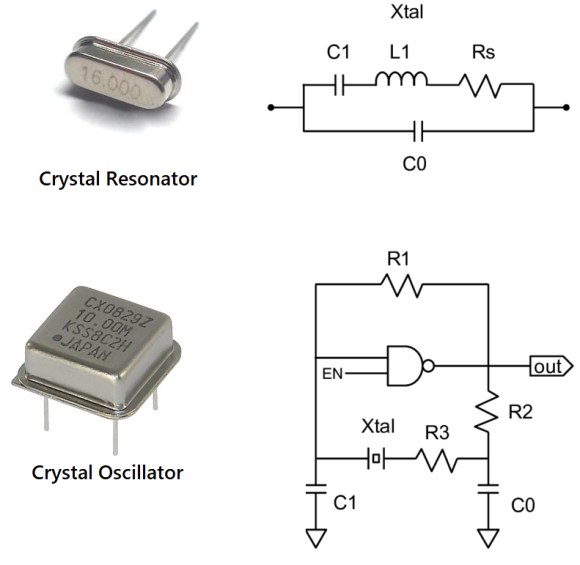
- If LFXT1CLK is used and needs precise timings, use a good clock crystal/TCXO/clock source.
- Use proper capacitance value for LFXT1CLK when an external crystal is used.
- Unused clock sources should be disabled to reduce power consumption.
- Pins that connect with external clock sources should be set as inputs if they are not used.
- Add a system start up delay of about 10 – 100ms to allow stabilization of clock sources.
- Clock outputs are available only in certain pins. If used, they are needed to be set accordingly.
- Use oscillator fault interrupt if needed. This becomes extremely necessary to ensure fail-safe clock operation when external clock sources are used alongside internal clock sources.
- For time sensitive hardware like timers, try to use a reliable clock source.
- Check for warnings in GRACE.
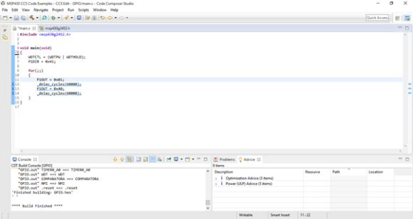
Code Example
#include <msp430.h>
void BCSplus_graceInit(void);
void GPIO_graceInit(void);
void WDTplus_graceInit(void);
void System_graceInit(void);
void main(void)
{
/* Stop watchdog timer from timing out during initial start-up. */
WDTCTL = WDTPW | WDTHOLD;
/* initialize Config for the MSP430 GPIO */
GPIO_graceInit();
/* initialize Config for the MSP430 2xx family clock systems (BCS) */
BCSplus_graceInit();
/* initialize Config for the MSP430 System Registers */
System_graceInit();
/* initialize Config for the MSP430 WDT+ */
WDTplus_graceInit();
while(1)
{
P1OUT ^= BIT6;
_delay_cycles(1);
};
}
void BCSplus_graceInit(void)
{
/* USER CODE START (section: BCSplus_graceInit_prologue) */
/* User initialization code */
/* USER CODE END (section: BCSplus_graceInit_prologue) */
/*
* Basic Clock System Control 2
*
* SELM_0 -- DCOCLK
* DIVM_1 -- Divide by 2
* SELS -- XT2CLK when XT2 oscillator present. LFXT1CLK or VLOCLK when XT2 oscillator not present
* DIVS_3 -- Divide by 8
* ~DCOR -- DCO uses internal resistor
*
* Note: ~DCOR indicates that DCOR has value zero
*/
BCSCTL2 = SELM_0 | DIVM_1 | SELS | DIVS_3;
if (CALBC1_1MHZ != 0xFF) {
/* Follow recommended flow. First, clear all DCOx and MODx bits. Then
* apply new RSELx values. Finally, apply new DCOx and MODx bit values.
*/
DCOCTL = 0x00;
BCSCTL1 = CALBC1_1MHZ; /* Set DCO to 1MHz */
DCOCTL = CALDCO_1MHZ;
}
/*
* Basic Clock System Control 1
*
* XT2OFF -- Disable XT2CLK
* ~XTS -- Low Frequency
* DIVA_0 -- Divide by 1
*
* Note: ~XTS indicates that XTS has value zero
*/
BCSCTL1 |= XT2OFF | DIVA_0;
/*
* Basic Clock System Control 3
*
* XT2S_0 -- 0.4 - 1 MHz
* LFXT1S_2 -- If XTS = 0, XT1 = VLOCLK ; If XTS = 1, XT1 = 3 - 16-MHz crystal or resonator
* XCAP_1 -- ~6 pF
*/
BCSCTL3 = XT2S_0 | LFXT1S_2 | XCAP_1;
/* USER CODE START (section: BCSplus_graceInit_epilogue) */
/* User code */
/* USER CODE END (section: BCSplus_graceInit_epilogue) */
}
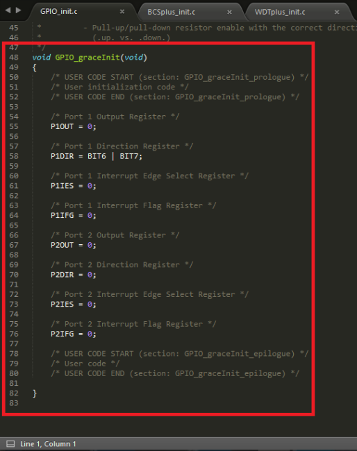
void GPIO_graceInit(void)
{
/* USER CODE START (section: GPIO_graceInit_prologue) */
/* User initialization code */
/* USER CODE END (section: GPIO_graceInit_prologue) */
/* Port 1 Output Register */
P1OUT = 0;
/* Port 1 Port Select Register */
P1SEL = BIT0 | BIT4;
/* Port 1 Direction Register */
P1DIR = BIT0 | BIT4 | BIT6;
/* Port 1 Interrupt Edge Select Register */
P1IES = 0;
/* Port 1 Interrupt Flag Register */
P1IFG = 0;
/* Port 2 Output Register */
P2OUT = 0;
/* Port 2 Direction Register */
P2DIR = 0;
/* Port 2 Interrupt Edge Select Register */
P2IES = 0;
/* Port 2 Interrupt Flag Register */
P2IFG = 0;
/* Port 3 Output Register */
P3OUT = 0;
/* Port 3 Direction Register */
P3DIR = 0;
/* USER CODE START (section: GPIO_graceInit_epilogue) */
/* User code */
/* USER CODE END (section: GPIO_graceInit_epilogue) */
}
void WDTplus_graceInit(void)
{
/* USER CODE START (section: RTC_B_graceInit_prologue) */
/* User initialization code */
/* USER CODE END (section: RTC_B_graceInit_prologue) */
/*
* WDTCTL, Watchdog Timer+ Register
*
* WDTPW -- Watchdog password
* WDTHOLD -- Watchdog timer+ is stopped
* ~WDTNMIES -- NMI on rising edge
* ~WDTNMI -- Reset function
* ~WDTTMSEL -- Watchdog mode
* ~WDTCNTCL -- No action
* ~WDTSSEL -- SMCLK
* ~WDTIS0 -- Watchdog clock source bit0 disabled
* ~WDTIS1 -- Watchdog clock source bit1 disabled
*
* Note: ~<BIT> indicates that <BIT> has value zero
*/
WDTCTL = WDTPW | WDTHOLD;
/* USER CODE START (section: RTC_B_graceInit_epilogue) */
/* User code */
/* USER CODE END (section: RTC_B_graceInit_epilogue) */
}
void System_graceInit(void)
{
/* USER CODE START (section: System_graceInit_prologue) */
/* User initialization code */
/* USER CODE END (section: System_graceInit_prologue) */
/* Clear oscillator fault flag with software delay */
do
{
// Clear OSC fault flag
IFG1 &= ~OFIFG;
// 50us delay
__delay_cycles(25);
} while (IFG1 & OFIFG);
/*
* SR, Status Register
*
* ~SCG1 -- Disable System clock generator 1
* ~SCG0 -- Disable System clock generator 0
* ~OSCOFF -- Oscillator On
* ~CPUOFF -- CPU On
* GIE -- General interrupt enable
*
* Note: ~<BIT> indicates that <BIT> has value zero
*/
__bis_SR_register(GIE);
/* USER CODE START (section: System_graceInit_epilogue) */
/* User code */
/* USER CODE END (section: System_graceInit_epilogue) */
}
Simulation
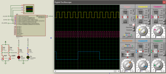
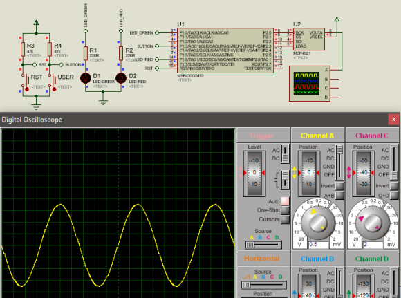
![BCSP Simulation]()
Explanation
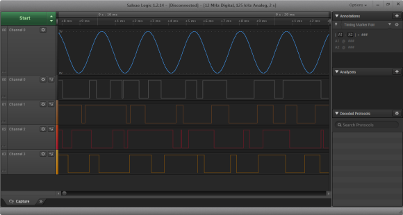
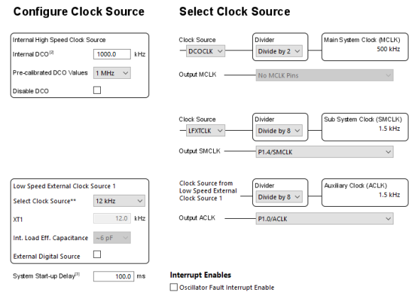
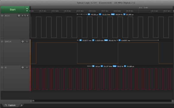
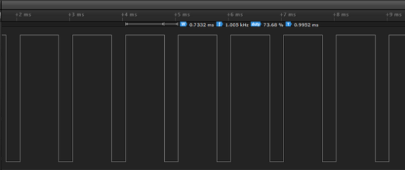
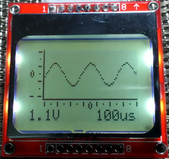
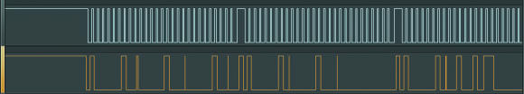
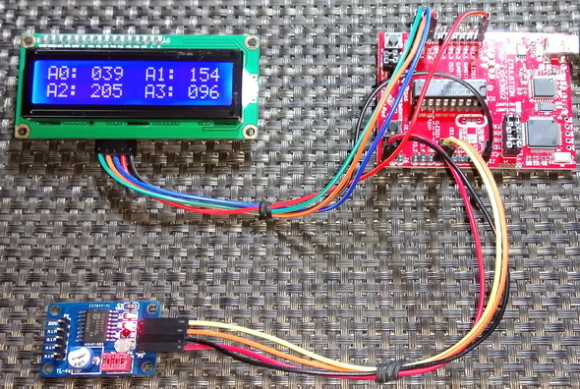
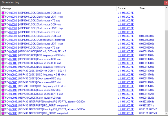
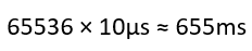
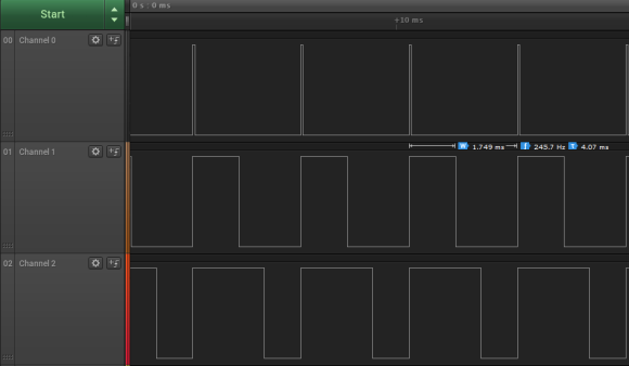
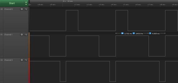
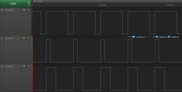
The demo example here is primarily used to extract SMCLK and ACLK signals. Here we just verified if these signals are as they are supposed to be. Using GRACE, we set MCLK 500 kHz, SMCLK 1500 Hz and ACLK 12 kHz. Clock outputs are obtained from respective pins as shown in the snap. The only thing additional here (not shown) is the P1.6 digital I/O. In the code, this I/O is toggled every one CPU cycle. It is not an indicator of CPU clock speed but just a test of I/O toggling speed for. MCLK has no output associated with it and so we can’t see its signal.
One major thing to note is the power supply voltage level. This is so because DCOCLK is dependent on VDD level. For low VDD voltages, high frequency oscillation generation is not possible. We have to remember that MSP430s are energy efficient devices and so there is always a trade-off between operating frequency and operating power consumption.
Another odd but important thing you may notice is the fact that the VDD value in MSP430 Launchpads is 3.6V instead of the more commonly used 3.3V. This is the maximum recommended VDD value although MSP430s can tolerate voltages up to 4.0V.
![GRACE Settings]()
Oscillators may show deviations in frequency due to changes in ambient temperature conditions. This in turn may affect communication and timing-related tasks.
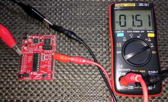
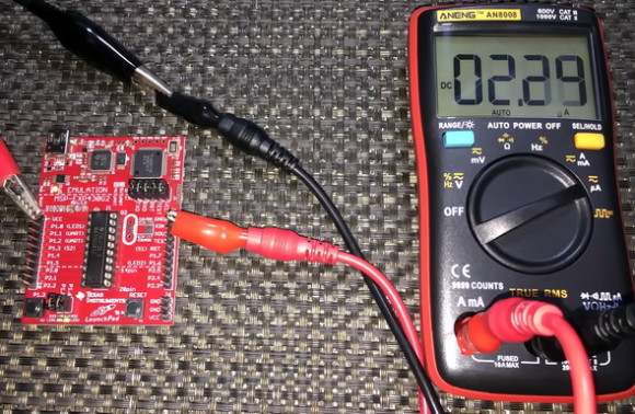
Demo
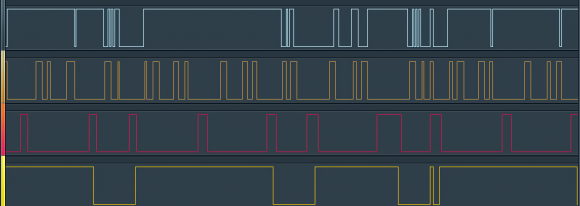
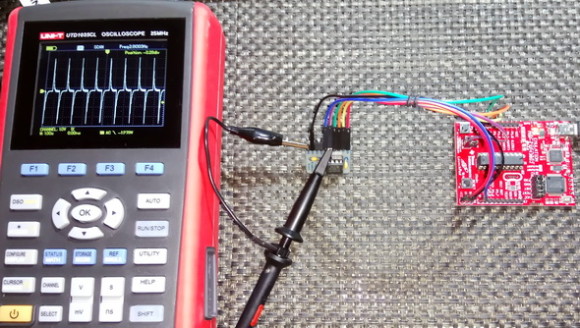
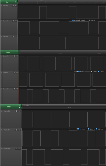
![BCSP]()
![Saleae Logic Screenshot]()
Demo video: https://www.youtube.com/watch?v=gHDibVxfegU.
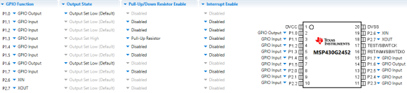
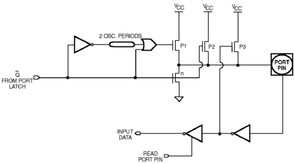
Digital I/Os (DIO)
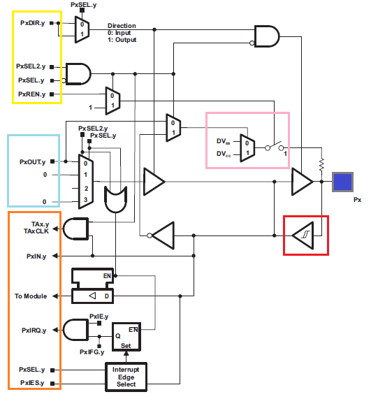
MSP430s, just like any micro, have digital I/Os for general-purpose input-output operations. The resources and features of MSP430 digital I/Os are very rich and more or less comparable to a typical ARM microcontroller. All I/O can be independently programmed. Many I/Os have external interrupt feature. Another cool feature is the availability of both internal pull-up and pull-down resistors for all I/Os and they can be individually and independently set. Additionally, many I/Os have alternate roles for communication buses, clock, etc. However, the digital I/Os are not 5V tolerant and we must be careful interfacing external devices with our MSP430 chips. I strongly recommend using some form of logic-level conversion circuitry in such cases.
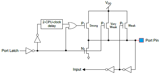
![Block Diagram]()
Typically, there are four major components in a digital I/O as highlighted in the block diagram above. The yellow region is responsible for setting I/O properties, the light blue area is dedicated for output functionalities, the orange area for inputs and external interrupts, the pink zone for internal pull resistors and finally the red area signifying the presence of a Schmitt trigger input stage which is very useful for noisy environments.
Code Example
#include <msp430g2452.h>
void GPIO_graceInit(void);
void BCSplus_graceInit(void);
void WDTplus_graceInit(void);
void System_graceInit(void);
void main(void)
{
/* Stop watchdog timer from timing out during initial start-up. */
WDTCTL = WDTPW | WDTHOLD;
/* initialize Config for the MSP430 GPIO */
GPIO_graceInit();
/* initialize Config for the MSP430 2xx family clock systems (BCS) */
BCSplus_graceInit();
/* initialize Config for the MSP430 System Registers */
System_graceInit();
/* initialize Config for the MSP430 WDT+ */
WDTplus_graceInit();
for(;;)
{
if((P1IN & BIT3) == !BIT3)
{
P1OUT |= BIT0;
_delay_cycles(40000);
P1OUT &= ~BIT0;
}
P1OUT ^= BIT6;
_delay_cycles(30000);
}
}
void BCSplus_graceInit(void)
{
/* USER CODE START (section: BCSplus_graceInit_prologue) */
/* User initialization code */
/* USER CODE END (section: BCSplus_graceInit_prologue) */
/*
* Basic Clock System Control 2
*
* SELM_0 -- DCOCLK
* DIVM_0 -- Divide by 1
* ~SELS -- DCOCLK
* DIVS_0 -- Divide by 1
* ~DCOR -- DCO uses internal resistor
*
* Note: ~<BIT> indicates that <BIT> has value zero
*/
BCSCTL2 = SELM_0 | DIVM_0 | DIVS_0;
if (CALBC1_1MHZ != 0xFF) {
/* Follow recommended flow. First, clear all DCOx and MODx bits. Then
* apply new RSELx values. Finally, apply new DCOx and MODx bit values.
*/
DCOCTL = 0x00;
BCSCTL1 = CALBC1_1MHZ; /* Set DCO to 1MHz */
DCOCTL = CALDCO_1MHZ;
}
/*
* Basic Clock System Control 1
*
* XT2OFF -- Disable XT2CLK
* ~XTS -- Low Frequency
* DIVA_0 -- Divide by 1
*
* Note: ~XTS indicates that XTS has value zero
*/
BCSCTL1 |= XT2OFF | DIVA_0;
/*
* Basic Clock System Control 3
*
* XT2S_0 -- 0.4 - 1 MHz
* LFXT1S_2 -- If XTS = 0, XT1 = VLOCLK ; If XTS = 1, XT1 = 3 - 16-MHz crystal or resonator
* XCAP_1 -- ~6 pF
*/
BCSCTL3 = XT2S_0 | LFXT1S_2 | XCAP_1;
/* USER CODE START (section: BCSplus_graceInit_epilogue) */
/* User code */
/* USER CODE END (section: BCSplus_graceInit_epilogue) */
}
void GPIO_graceInit(void)
{
/* USER CODE START (section: GPIO_graceInit_prologue) */
/* User initialization code */
/* USER CODE END (section: GPIO_graceInit_prologue) */
/* Port 1 Output Register */
P1OUT = BIT3;
/* Port 1 Direction Register */
P1DIR = BIT0 | BIT6;
/* Port 1 Resistor Enable Register */
P1REN = BIT3;
/* Port 1 Interrupt Edge Select Register */
P1IES = 0;
/* Port 1 Interrupt Flag Register */
P1IFG = 0;
/* Port 2 Output Register */
P2OUT = 0;
/* Port 2 Direction Register */
P2DIR = 0;
/* Port 2 Interrupt Edge Select Register */
P2IES = 0;
/* Port 2 Interrupt Flag Register */
P2IFG = 0;
/* USER CODE START (section: GPIO_graceInit_epilogue) */
/* User code */
/* USER CODE END (section: GPIO_graceInit_epilogue) */
}
void System_graceInit(void)
{
/* USER CODE START (section: System_graceInit_prologue) */
/* User initialization code */
/* USER CODE END (section: System_graceInit_prologue) */
/* Clear oscillator fault flag with software delay */
do
{
// Clear OSC fault flag
IFG1 &= ~OFIFG;
// 50us delay
__delay_cycles(50);
} while (IFG1 & OFIFG);
/*
* SR, Status Register
*
* ~SCG1 -- Disable System clock generator 1
* ~SCG0 -- Disable System clock generator 0
* ~OSCOFF -- Oscillator On
* ~CPUOFF -- CPU On
* GIE -- General interrupt enable
*
* Note: ~<BIT> indicates that <BIT> has value zero
*/
__bis_SR_register(GIE);
/* USER CODE START (section: System_graceInit_epilogue) */
/* User code */
/* USER CODE END (section: System_graceInit_epilogue) */
}
void WDTplus_graceInit(void)
{
/* USER CODE START (section: RTC_B_graceInit_prologue) */
/* User initialization code */
/* USER CODE END (section: RTC_B_graceInit_prologue) */
/*
* WDTCTL, Watchdog Timer+ Register
*
* WDTPW -- Watchdog password
* WDTHOLD -- Watchdog timer+ is stopped
* ~WDTNMIES -- NMI on rising edge
* ~WDTNMI -- Reset function
* ~WDTTMSEL -- Watchdog mode
* ~WDTCNTCL -- No action
* ~WDTSSEL -- SMCLK
* ~WDTIS0 -- Watchdog clock source bit0 disabled
* ~WDTIS1 -- Watchdog clock source bit1 disabled
*
* Note: ~<BIT> indicates that <BIT> has value zero
*/
WDTCTL = WDTPW | WDTHOLD;
/* USER CODE START (section: RTC_B_graceInit_epilogue) */
/* User code */
/* USER CODE END (section: RTC_B_graceInit_epilogue) */
}
Simulation
![DIO Simulation]()
Explanation
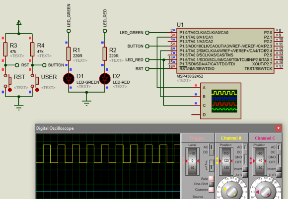
The most classical “Hello World” demo for digital I/Os is blinking a LED. Here I demonstrated the same but with some minor differences. Here Launchpad board’s user button and LEDs are used. LED connected to P1.6 blinks continuously while P1.0 LED blinks only when the user button is pressed, slowing down P1.6 LED’s blink rate. Note _delay_cycles were used to create software delays.
![Grace Setting]()
At this stage I must point out, some basic rules that we must follow when we use digital I/Os of MSP430s:
- Unused I/Os should be declared as inputs or they should be externally pulled to VDD/VSS.
- Unused digital I/Os can be left unconnected and floating although it is not wise to do so.
- The same applies for oscillator pins. By default, GRACE treats them as oscillator pins.
- I/Os are not 5V tolerant. Some sort of mechanism must be applied when using 5V devices.
- Most I/Os have more than one function and so be aware of conflicts.
- When driving large loads with I/O, use external components like BJTs, FETs, drivers, etc.
- When using GRACE, be sure of the IC package you are using.
- When external pull resistor is present, do not use the internal ones and vice versa.
- Explore your device’s datasheet for I/O features and limits although most are common.
Demo
![DIO Demo]()
Demo video: https://www.youtube.com/watch?v=fWlNiEZk4iM.
External Interrupts (EXTI)
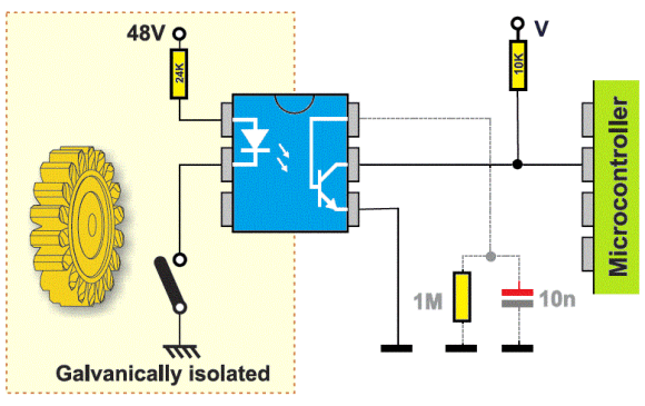
External interrupt is an extended feature of digital I/Os in input mode. External interrupts make a micro to respond instantly to changes done on it digital input pin(s) by an external event(s)/trigger(s), skipping other tasks. Such interrupts are useful in a wide variety of applications. In case of low power energy efficient micros like the MSP430s, interrupts as such can be used to bring a micro out of sleep mode. In other words, an external interrupt acts like a wakeup call. For example, it is extremely important to conserve very limited battery energy in a TV remote controller while at the same time it is also necessary to keep it completely responsive to button presses. Thus, we need to put its host micro in sleep mode when we are not using it and make it respond to button presses immediately when any button is pressed. A MSP430 micro in sleep/idle mode consumes literally no energy at all and that is why they are the best micros for battery-backed low power applications.
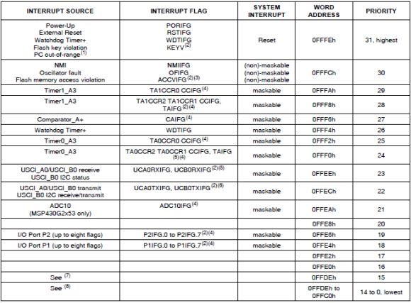
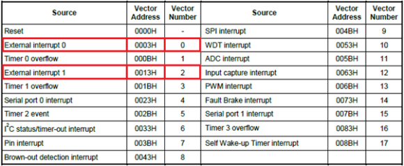
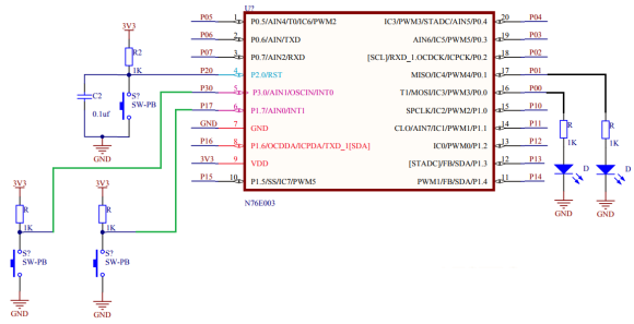
![Interrupt Vectors]()
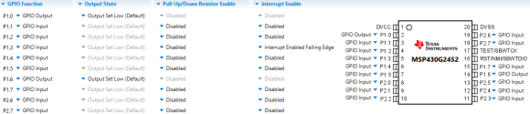
Fortunately for us, most MSP430G2xx digital I/Os have external interrupt handling capability – a much desired feature. Shown above is the interrupt map for MSP430G2553. Note external interrupts are maskable interrupts and have low priority compares to other interrupts. We must consider this fact when coding a multi-interrupt-based application.
Code Example
#include <MSP430G2452.h>
unsigned char state = 0x00;
void BCSplus_graceInit(void);
void GPIO_graceInit(void);
void System_graceInit(void);
void WDTplus_graceInit(void);
#pragma vector=PORT1_VECTOR
__interrupt void PORT1_ISR_HOOK(void)
{
state = ~state;
P1OUT ^= BIT0;
P1IFG = 0x00;
}
void main(void)
{
/* Stop watchdog timer from timing out during initial start-up. */
WDTCTL = WDTPW | WDTHOLD;
/* initialize Config for the MSP430 GPIO */
GPIO_graceInit();
/* initialize Config for the MSP430 2xx family clock systems (BCS) */
BCSplus_graceInit();
/* initialize Config for the MSP430 System Registers */
System_graceInit();
/* initialize Config for the MSP430 WDT+ */
WDTplus_graceInit();
do
{
P1OUT ^= BIT6;
if(state)
{
_delay_cycles(60000);
}
else
{
_delay_cycles(30000);
}
}while(1);
}
void BCSplus_graceInit(void)
{
/* USER CODE START (section: BCSplus_graceInit_prologue) */
/* User initialization code */
/* USER CODE END (section: BCSplus_graceInit_prologue) */
/*
* Basic Clock System Control 2
*
* SELM_0 -- DCOCLK
* DIVM_0 -- Divide by 1
* ~SELS -- DCOCLK
* DIVS_0 -- Divide by 1
* ~DCOR -- DCO uses internal resistor
*
* Note: ~<BIT> indicates that <BIT> has value zero
*/
BCSCTL2 = SELM_0 | DIVM_0 | DIVS_0;
if (CALBC1_1MHZ != 0xFF) {
/* Follow recommended flow. First, clear all DCOx and MODx bits. Then
* apply new RSELx values. Finally, apply new DCOx and MODx bit values.
*/
DCOCTL = 0x00;
BCSCTL1 = CALBC1_1MHZ; /* Set DCO to 1MHz */
DCOCTL = CALDCO_1MHZ;
}
/*
* Basic Clock System Control 1
*
* XT2OFF -- Disable XT2CLK
* ~XTS -- Low Frequency
* DIVA_0 -- Divide by 1
*
* Note: ~XTS indicates that XTS has value zero
*/
BCSCTL1 |= XT2OFF | DIVA_0;
/*
* Basic Clock System Control 3
*
* XT2S_0 -- 0.4 - 1 MHz
* LFXT1S_2 -- If XTS = 0, XT1 = VLOCLK ; If XTS = 1, XT1 = 3 - 16-MHz crystal or resonator
* XCAP_1 -- ~6 pF
*/
BCSCTL3 = XT2S_0 | LFXT1S_2 | XCAP_1;
/* USER CODE START (section: BCSplus_graceInit_epilogue) */
/* User code */
/* USER CODE END (section: BCSplus_graceInit_epilogue) */
}
void GPIO_graceInit(void)
{
/* USER CODE START (section: GPIO_graceInit_prologue) */
/* User initialization code */
/* USER CODE END (section: GPIO_graceInit_prologue) */
/* Port 1 Output Register */
P1OUT = 0;
/* Port 1 Direction Register */
P1DIR = BIT0 | BIT6;
/* Port 1 Interrupt Edge Select Register */
P1IES = BIT3;
/* Port 1 Interrupt Flag Register */
P1IFG = 0;
/* Port 1 Interrupt Enable Register */
P1IE = BIT3;
/* Port 2 Output Register */
P2OUT = 0;
/* Port 2 Port Select Register */
P2SEL &= ~(BIT6 | BIT7);
/* Port 2 Direction Register */
P2DIR = 0;
/* Port 2 Interrupt Edge Select Register */
P2IES = 0;
/* Port 2 Interrupt Flag Register */
P2IFG = 0;
/* USER CODE START (section: GPIO_graceInit_epilogue) */
/* User code */
/* USER CODE END (section: GPIO_graceInit_epilogue) */
}
void System_graceInit(void)
{
/* USER CODE START (section: System_graceInit_prologue) */
/* User initialization code */
/* USER CODE END (section: System_graceInit_prologue) */
/* Clear oscillator fault flag with software delay */
do
{
// Clear OSC fault flag
IFG1 &= ~OFIFG;
// 50us delay
__delay_cycles(50);
} while (IFG1 & OFIFG);
/*
* SR, Status Register
*
* ~SCG1 -- Disable System clock generator 1
* ~SCG0 -- Disable System clock generator 0
* ~OSCOFF -- Oscillator On
* ~CPUOFF -- CPU On
* GIE -- General interrupt enable
*
* Note: ~<BIT> indicates that <BIT> has value zero
*/
__bis_SR_register(GIE);
/* USER CODE START (section: System_graceInit_epilogue) */
/* User code */
/* USER CODE END (section: System_graceInit_epilogue) */
}
void WDTplus_graceInit(void)
{
/* USER CODE START (section: RTC_B_graceInit_prologue) */
/* User initialization code */
/* USER CODE END (section: RTC_B_graceInit_prologue) */
/*
* WDTCTL, Watchdog Timer+ Register
*
* WDTPW -- Watchdog password
* WDTHOLD -- Watchdog timer+ is stopped
* ~WDTNMIES -- NMI on rising edge
* ~WDTNMI -- Reset function
* ~WDTTMSEL -- Watchdog mode
* ~WDTCNTCL -- No action
* ~WDTSSEL -- SMCLK
* ~WDTIS0 -- Watchdog clock source bit0 disabled
* ~WDTIS1 -- Watchdog clock source bit1 disabled
*
* Note: ~<BIT> indicates that <BIT> has value zero
*/
WDTCTL = WDTPW | WDTHOLD;
/* USER CODE START (section: RTC_B_graceInit_epilogue) */
/* User code */
/* USER CODE END (section: RTC_B_graceInit_epilogue) */
}
Simulation
![EXTI Simulation]()
Explanation
The basic theme and the hardware setup for this demo is same as that of the previous one. The only difference is the Launchpad user button. Rather than using polling method, external interrupt method is used. When P1.3 detects a falling edge, P1.0’s state is altered while P1.6 toggles independently in the main loop, denoting two separate independent processes at work simultaneously. Every external interrupt changes the toggle speed of P1.6 LED.
![Grace Settings]()
Demo
![EXTI]()
Demo video: https://www.youtube.com/watch?v=LlTvj-CSiBE.
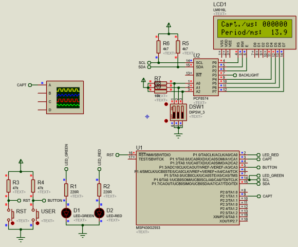
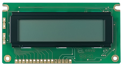
Alphanumeric LCD
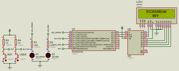
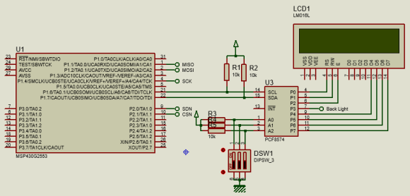
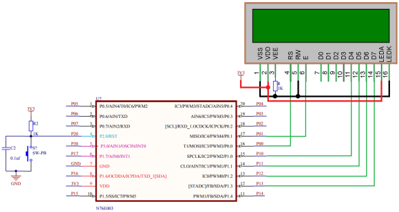
Alphanumeric LCDs are popular for projecting data and information quickly and efficiently. To use them, we do not need any additional hardware feature in a micro. Digital I/Os are what we need to use these displays.
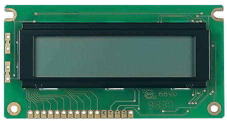
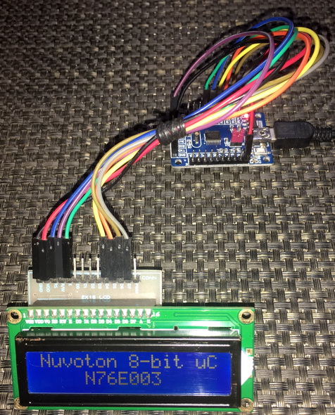
![LCD]()
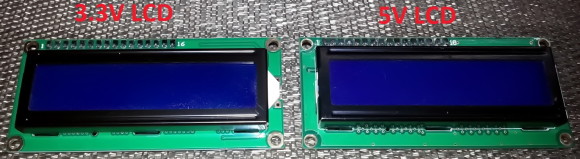
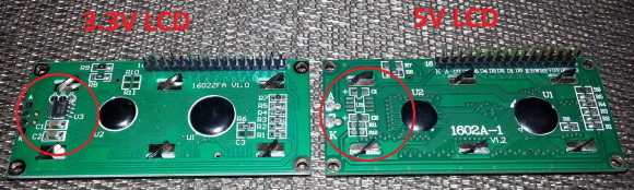
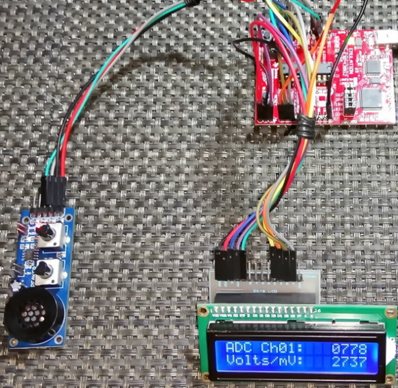
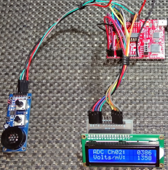
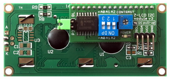
Usually to use these LCDs we need 5V power supply. 3.3V versions of these LCD are rare on the other hand. It is, however, possible to power up 5V version LCDs with 5V supply while using 3.3V logic for communication. In TTL logic, something above 2.8V is just above the minimum allowed logic high voltage. When VDD is less than 3V, it, then, becomes necessary to use logic level conversion circuitry. Here in my demo I used a 3.3V version LCD to keep things simple and tidy. Shown below are LCDs for different voltage levels. Both LCDs look same but if you check the backside of both LCDs you’ll notice a difference. In the 3.3V version LCD, there are some additional components present, notably an 8 pin SMD IC. This is a ICL7660 negative voltage generator IC.
![Seeeduino LCD (1)]()
![Seeeduino LCD (2)]()
Similarly, alphanumeric LCDs also have operating frequency limit. Usually it is about 250 kHz. Refer to the datasheet of the LCD you are using. If the digital I/Os are faster than this max limit value, it is highly likely that the LCD won’t show any valid data at all or it will show up garbage characters. To counter this issue, either we have to use a low MCU clock frequency or add some delays in our LCD library to slow the processes down.
Software delays are often required to introduce time delays in a code. Such delays will be needed for the LCD library. As discussed before by default, CCS doesn’t provide delay time functions i.e. delay milliseconds (delay_ms) and delay micro-seconds (delay_us). Instead it provides _delay_cycles function for delays. Most of us will not be comfortable with delay cycles function as it doesn’t directly signify the amount of time wasted. Thus, delay time functions are musts. Although software delays are inefficient in terms of coding and performance, they are helpful in debugging stuffs quickly in a rudimentary fashion. A much novel and precise approach of creating time delays is achieved using a timer. In this example, we will need both LCD and delay libraries. I already showed how to incorporate custom libraries in a CCS Project and here I implemented that addition.
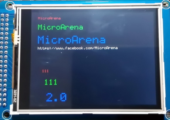
There are other types of displays in the realm of LCDs. These include monochrome graphical LCDs, TFT LCDs, OLED LCDs, etc. However, it is literally impossible to integrate these displays with MSP430G2xx micros. Firstly, this is so due to low memories and secondly due to low pin counts. MSP430G2xx micros are also not as fast as ARM micros. Speed plays a vital role in processing graphics.
![TFT LCD]()
Code Example
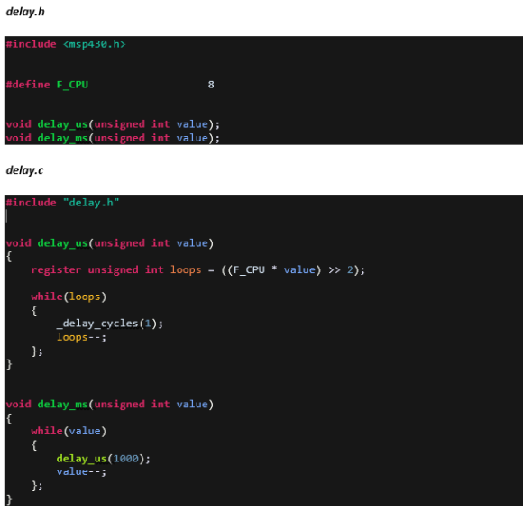
delay.h
#include <msp430.h>
#define F_CPU 8
void delay_us(unsigned int value);
void delay_ms(unsigned int value);
delay.c
#include "delay.h"
void delay_us(unsigned int value)
{
register unsigned int loops = ((F_CPU * value) >> 2) ;
while(loops)
{
_delay_cycles(1);
loops--;
};
}
void delay_ms(unsigned int value)
{
while(value)
{
delay_us(1000);
value--;
};
}
lcd.h
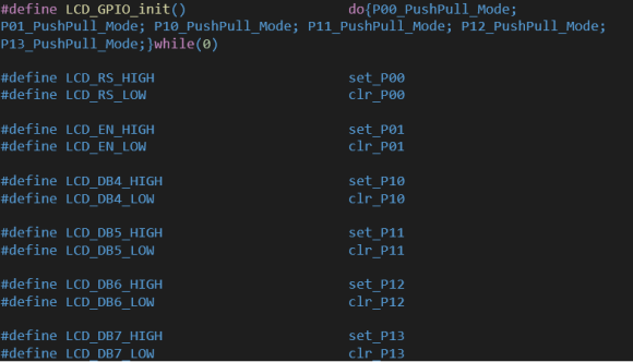
#include <msp430.h>
#include <delay.h>
#define LCD_PORT P2OUT
#define LCD_RS BIT0
#define LCD_EN BIT1
#define LCD_DB4 BIT2
#define LCD_DB5 BIT3
#define LCD_DB6 BIT4
#define LCD_DB7 BIT5
#define LCD_RS_HIGH LCD_PORT |= LCD_RS
#define LCD_RS_LOW LCD_PORT &= ~LCD_RS
#define LCD_EN_HIGH LCD_PORT |= LCD_EN
#define LCD_EN_LOW LCD_PORT &= ~LCD_EN
#define LCD_DB4_HIGH LCD_PORT |= LCD_DB4
#define LCD_DB4_LOW LCD_PORT &= ~LCD_DB4
#define LCD_DB5_HIGH LCD_PORT |= LCD_DB5
#define LCD_DB5_LOW LCD_PORT &= ~LCD_DB5
#define LCD_DB6_HIGH LCD_PORT |= LCD_DB6
#define LCD_DB6_LOW LCD_PORT &= ~LCD_DB6
#define LCD_DB7_HIGH LCD_PORT |= LCD_DB7
#define LCD_DB7_LOW LCD_PORT &= ~LCD_DB7
#define clear_display 0x01
#define goto_home 0x02
#define cursor_direction_inc (0x04 | 0x02)
#define cursor_direction_dec (0x04 | 0x00)
#define display_shift (0x04 | 0x01)
#define display_no_shift (0x04 | 0x00)
#define display_on (0x08 | 0x04)
#define display_off (0x08 | 0x02)
#define cursor_on (0x08 | 0x02)
#define cursor_off (0x08 | 0x00)
#define blink_on (0x08 | 0x01)
#define blink_off (0x08 | 0x00)
#define _8_pin_interface (0x20 | 0x10)
#define _4_pin_interface (0x20 | 0x00)
#define _2_row_display (0x20 | 0x08)
#define _1_row_display (0x20 | 0x00)
#define _5x10_dots (0x20 | 0x40)
#define _5x7_dots (0x20 | 0x00)
#define DAT 1
#define CMD 0
void LCD_init(void);
void LCD_send(unsigned char value, unsigned char mode);
void LCD_4bit_send(unsigned char lcd_data);
void LCD_putstr(char *lcd_string);
void LCD_putchar(char char_data);
void LCD_clear_home(void);
void LCD_goto(unsigned char x_pos, unsigned char y_pos);
void toggle_EN_pin(void);
void toggle_io(unsigned char lcd_data, unsigned char bit_pos, unsigned char pin_num);
lcd.c
#include "lcd.h"
void LCD_init(void)
{
LCD_PORT |= (LCD_RS | LCD_EN | LCD_DB4 | LCD_DB5 | LCD_DB6 | LCD_DB7);
delay_ms(20);
toggle_EN_pin();
LCD_RS_LOW;
LCD_DB7_LOW;
LCD_DB6_LOW;
LCD_DB5_HIGH;
LCD_DB4_HIGH;
toggle_EN_pin();
LCD_DB7_LOW;
LCD_DB6_LOW;
LCD_DB5_HIGH;
LCD_DB4_HIGH;
toggle_EN_pin();
LCD_DB7_LOW;
LCD_DB6_LOW;
LCD_DB5_HIGH;
LCD_DB4_HIGH;
toggle_EN_pin();
LCD_DB7_LOW;
LCD_DB6_LOW;
LCD_DB5_HIGH;
LCD_DB4_LOW;
toggle_EN_pin();
LCD_send((_4_pin_interface | _2_row_display | _5x7_dots), CMD);
LCD_send((display_on | cursor_off | blink_off), CMD);
LCD_send(clear_display, CMD);
LCD_send((cursor_direction_inc | display_no_shift), CMD);
}
void LCD_send(unsigned char value, unsigned char mode)
{
switch(mode)
{
case DAT:
{
LCD_RS_HIGH;
break;
}
case CMD:
{
LCD_RS_LOW;
break;
}
}
LCD_4bit_send(value);
}
void LCD_4bit_send(unsigned char lcd_data)
{
toggle_io(lcd_data, 7, LCD_DB7);
toggle_io(lcd_data, 6, LCD_DB6);
toggle_io(lcd_data, 5, LCD_DB5);
toggle_io(lcd_data, 4, LCD_DB4);
toggle_EN_pin();
toggle_io(lcd_data, 3, LCD_DB7);
toggle_io(lcd_data, 2, LCD_DB6);
toggle_io(lcd_data, 1, LCD_DB5);
toggle_io(lcd_data, 0, LCD_DB4);
toggle_EN_pin();
}
void LCD_putstr(char *lcd_string)
{
do
{
LCD_send(*lcd_string++, DAT);
}while(*lcd_string != '\0');
}
void LCD_putchar(char char_data)
{
LCD_send(char_data, DAT);
}
void LCD_clear_home(void)
{
LCD_send(clear_display, CMD);
LCD_send(goto_home, CMD);
}
void LCD_goto(unsigned char x_pos, unsigned char y_pos)
{
if(y_pos == 0)
{
LCD_send((0x80 | x_pos), CMD);
}
else
{
LCD_send((0x80 | 0x40 | x_pos), CMD);
}
}
void toggle_EN_pin(void)
{
LCD_EN_HIGH;
delay_ms(2);
LCD_EN_LOW;
delay_ms(2);
}
void toggle_io(unsigned char lcd_data, unsigned char bit_pos, unsigned char pin_num)
{
unsigned char temp = 0x00;
temp = (0x01 & (lcd_data >> bit_pos));
switch(temp)
{
case 0:
{
LCD_PORT &= ~pin_num;
break;
}
default:
{
LCD_PORT |= pin_num;
break;
}
}
}
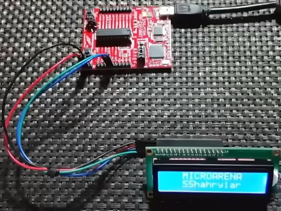
main.c
#include <msp430.h>
#include "delay.h"
#include "lcd.h"
void GPIO_graceInit(void);
void BCSplus_graceInit(void);
void System_graceInit(void);
void WDTplus_graceInit(void);
void main(void)
{
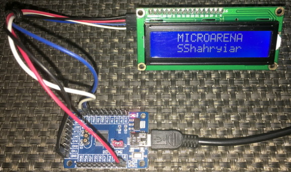
unsigned char s = 0;
const char txt1[] = {"MICROARENA"};
const char txt2[] = {"SShahryiar"};
const char txt3[] = {"MSP-EXP430G2"};
const char txt4[] = {"Launchpad!"};
/* Stop watchdog timer from timing out during initial start-up. */
WDTCTL = WDTPW | WDTHOLD;
/* initialize Config for the MSP430 GPIO */
GPIO_graceInit();
/* initialize Config for the MSP430 2xx family clock systems (BCS) */
BCSplus_graceInit();
/* initialize Config for the MSP430 System Registers */
System_graceInit();
/* initialize Config for the MSP430 WDT+ */
WDTplus_graceInit();
LCD_init();
LCD_clear_home();
LCD_goto(3, 0);
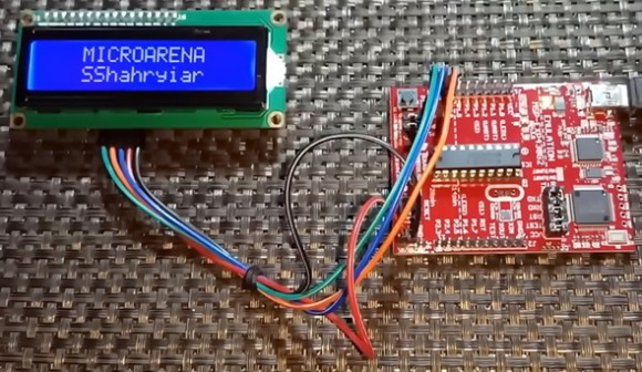
LCD_putstr(txt1);
LCD_goto(3, 1);
LCD_putstr(txt2);
delay_ms(2600);
LCD_clear_home();
for(s = 0; s < 12; s++)
{
LCD_goto((2 + s), 0);
LCD_putchar(txt3[s]);
delay_ms(90);
}
for(s = 0; s < 10; s++)
{
LCD_goto((3 + s), 1);
LCD_putchar(txt4[s]);
delay_ms(90);
}
while(1)
{
};
}
void GPIO_graceInit(void)
{
/* USER CODE START (section: GPIO_graceInit_prologue) */
/* User initialization code */
/* USER CODE END (section: GPIO_graceInit_prologue) */
/* Port 1 Output Register */
P1OUT = 0;
/* Port 1 Direction Register */
P1DIR = 0;
/* Port 1 Interrupt Edge Select Register */
P1IES = 0;
/* Port 1 Interrupt Flag Register */
P1IFG = 0;
/* Port 2 Output Register */
P2OUT = 0;
/* Port 2 Port Select Register */
P2SEL &= ~(BIT6 | BIT7);
/* Port 2 Direction Register */
P2DIR = BIT0 | BIT1 | BIT2 | BIT3 | BIT4 | BIT5;
/* Port 2 Interrupt Edge Select Register */
P2IES = 0;
/* Port 2 Interrupt Flag Register */
P2IFG = 0;
/* USER CODE START (section: GPIO_graceInit_epilogue) */
/* User code */
/* USER CODE END (section: GPIO_graceInit_epilogue) */
}
void BCSplus_graceInit(void)
{
/* USER CODE START (section: BCSplus_graceInit_prologue) */
/* User initialization code */
/* USER CODE END (section: BCSplus_graceInit_prologue) */
/*
* Basic Clock System Control 2
*
* SELM_0 -- DCOCLK
* DIVM_0 -- Divide by 1
* ~SELS -- DCOCLK
* DIVS_0 -- Divide by 1
* ~DCOR -- DCO uses internal resistor
*
* Note: ~<BIT> indicates that <BIT> has value zero
*/
BCSCTL2 = SELM_0 | DIVM_0 | DIVS_0;
if (CALBC1_8MHZ != 0xFF) {
/* Adjust this accordingly to your VCC rise time */
__delay_cycles(100000);
// Follow recommended flow. First, clear all DCOx and MODx bits. Then
// apply new RSELx values. Finally, apply new DCOx and MODx bit values.
DCOCTL = 0x00;
BCSCTL1 = CALBC1_8MHZ; /* Set DCO to 8MHz */
DCOCTL = CALDCO_8MHZ;
}
/*
* Basic Clock System Control 1
*
* XT2OFF -- Disable XT2CLK
* ~XTS -- Low Frequency
* DIVA_0 -- Divide by 1
*
* Note: ~XTS indicates that XTS has value zero
*/
BCSCTL1 |= XT2OFF | DIVA_0;
/*
* Basic Clock System Control 3
*
* XT2S_0 -- 0.4 - 1 MHz
* LFXT1S_0 -- If XTS = 0, XT1 = 32768kHz Crystal ; If XTS = 1, XT1 = 0.4 - 1-MHz crystal or resonator
* XCAP_1 -- ~6 pF
*/
BCSCTL3 = XT2S_0 | LFXT1S_0 | XCAP_1;
/* USER CODE START (section: BCSplus_graceInit_epilogue) */
/* User code */
/* USER CODE END (section: BCSplus_graceInit_epilogue) */
}
void System_graceInit(void)
{
/* USER CODE START (section: System_graceInit_prologue) */
/* User initialization code */
/* USER CODE END (section: System_graceInit_prologue) */
/*
* SR, Status Register
*
* ~SCG1 -- Disable System clock generator 1
* ~SCG0 -- Disable System clock generator 0
* ~OSCOFF -- Oscillator On
* ~CPUOFF -- CPU On
* GIE -- General interrupt enable
*
* Note: ~<BIT> indicates that <BIT> has value zero
*/
__bis_SR_register(GIE);
/* USER CODE START (section: System_graceInit_epilogue) */
/* User code */
/* USER CODE END (section: System_graceInit_epilogue) */
}
void WDTplus_graceInit(void)
{
/* USER CODE START (section: RTC_B_graceInit_prologue) */
/* User initialization code */
/* USER CODE END (section: RTC_B_graceInit_prologue) */
/*
* WDTCTL, Watchdog Timer+ Register
*
* WDTPW -- Watchdog password
* WDTHOLD -- Watchdog timer+ is stopped
* ~WDTNMIES -- NMI on rising edge
* ~WDTNMI -- Reset function
* ~WDTTMSEL -- Watchdog mode
* ~WDTCNTCL -- No action
* ~WDTSSEL -- SMCLK
* ~WDTIS0 -- Watchdog clock source bit0 disabled
* ~WDTIS1 -- Watchdog clock source bit1 disabled
*
* Note: ~<BIT> indicates that <BIT> has value zero
*/
WDTCTL = WDTPW | WDTHOLD;
/* USER CODE START (section: RTC_B_graceInit_epilogue) */
/* User code */
/* USER CODE END (section: RTC_B_graceInit_epilogue) */
}
Simulation
![LCD Simulation]()
Explanation
Hardly there is a thing to explain here. However, there are a few things to note. After having decided the CPU clock frequency, we must edit the following line of the delay header file to make our delays work as much as accurate as possible:
#define F_CPU 8 //CPU Clock in MHz
Software delays are not 100% accurate since they employ wasteful loops of delay cycles which in turn add extra CPU cycles. They are always somewhat close to the actual required value. Delays are also dependent on oscillator accuracy.
![grace]()
Though it is not mandatory but I still recommend that we try to use digital I/Os that have no or least alternate functionalities. This will ensure maximum utilization of limited resources and avoid conflicts as well. Here in this demo, I used P2 port just for that.
Choosing the right display for a project is often tedious. We have lot of options nowadays ranging from simple LED displays to TFT LCDs. However, considering low power consumption and limited resource availability, it wise to use the simplest form of display. If a project can be completed using seven segment displays, it wasteful and expensive to use a OLED display with seven segment fonts.
LCD displays host their own set of electronics and are prone to Electromagnetic Interference (EMI) and related issues. In many cases, one may end up having a EMI troubled LCD while having the host MCU fully functional and vice-versa. It is always wise to use a short path between a LCD and its host MCU. If needed, use passive low pass antialiasing filters.
Demo
![LCD Demo]()
Demo video: https://www.youtube.com/watch?v=sJF8oJPu18s.
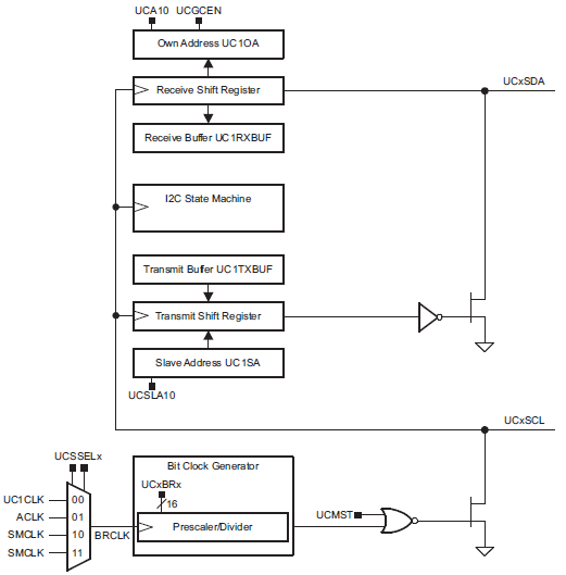
Timer Overview
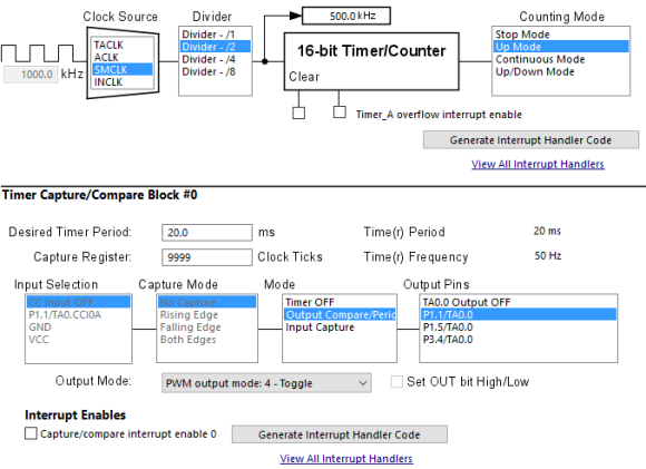
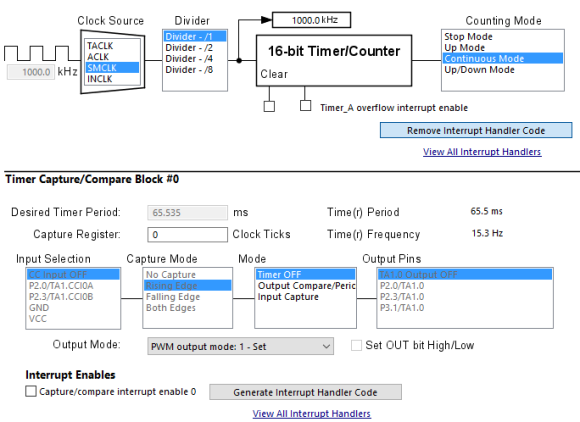
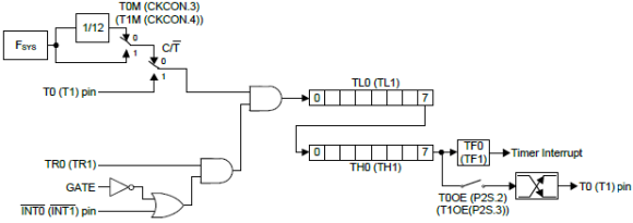
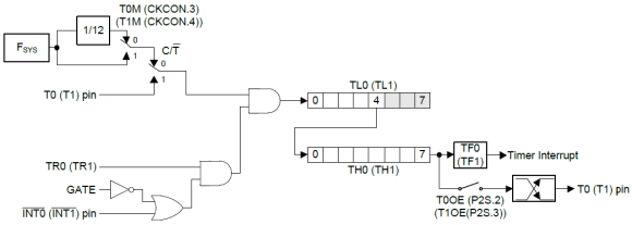
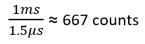
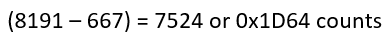
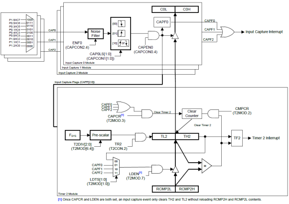
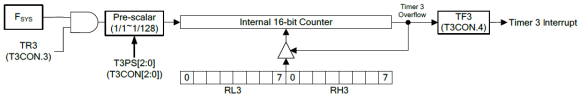
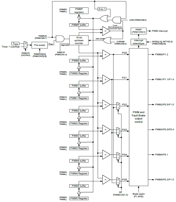
There are several types of timers in MSP430 micros. These include Watchdog Timer (WDT), Real Time Clock (RTC), Basic Timer 1 and Timer A and Timer B. Timer As and Bs are general purpose 16-bit timers that are suitable for time base generations, pulse width modulations (PWM) and input captures. the other three types have special uses and their names suggest their purposes. All MSP430 devices have at least one Timer A module and a WDT module. Since both are common amongst all devices, we will be studying about them here. Timer As and Bs are almost same. The difference between the two is the presence of some additional features like more Capture/Compare (CC) channels in Timer Bs.
Timer A
In TI’s literature, timers are named like Timer0_A3, Timer_B7, etc. A number can be present right after the word Timer in some case and in other cases, it may be absent. This number is present whenever there are multiple timers of same type in a MSP430 micro. For example, there are two Timer A3s in MSP430G2553 micros and so they are labelled as Timer0_A3 and Timer1_A3. The other number in the timer’s name after the timer type letter denotes the number of CC channels available with it.
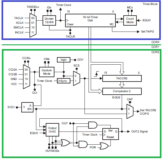
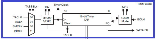
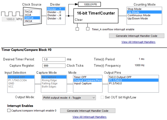
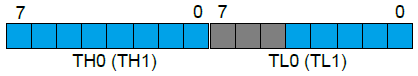
Shown below is the block diagram of Timer A module. MSP430G2452 has one and MSP430G2553 has two Timer A3 modules. Typically, in any micro’s timer we would expect two things – first a counter block (highlighted in purple) and second CC modules (highlighted in green). As we can see the CC channels share the same TAR register and so they share the similar properties.
![Block Diagram]()
The diagram below shows that clock sources we can use for a Timer A module. It can be clocked with two internal clock sources – ACLK and SMCLK or with two external clock sources – TACLK and INCLK. Actually, INCLK and TACLK are same but one is complementary of the other. These external clocks can be used to make the timer module work as counter.
![Counter Block Diagram]()
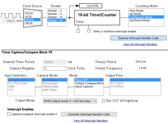
Next, we have a prescaler to scale down selected clock source followed by the counter block. What’s interesting about MSP430 timers is the counter’s mode of operation. There are four modes of counter operation and these modes define counting direction:
- Stop Mode
It is basically a hold state. All timer registers are retained and the timer is halted.
- Continuous Mode
In this mode, the timer counts up from 0 to top value (here 0xFFFF or 65535 in 16-bit Timer A3) and then rolls over to zero.
- Up Mode
This mode is same as continuous mode except for the top value. The top value of the timer is set by the value in TACCR0.
- Up/Down Mode
In this mode, the timer counts from 0 to TACCR0 value and then rolls back from that value to 0. The period of the timer is twice the TACCR0 counts.
Then we have timer interrupt just as in any other microcontroller.
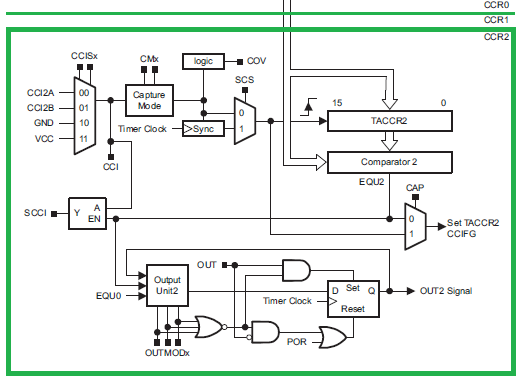
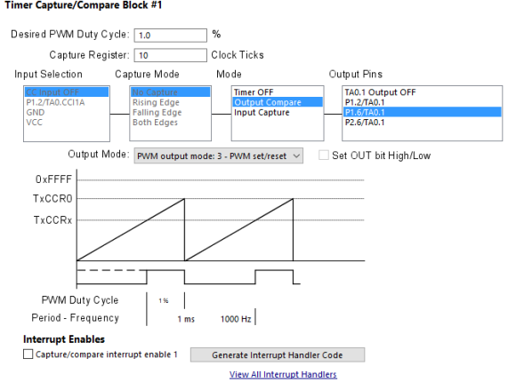
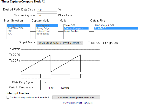
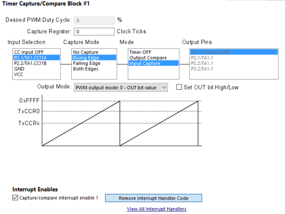
MSP430G2452 has one Timer A3 module and so it has three CC channels. Likewise, MSP430G2553 has six CC channels. When it comes to extreme engineering, TI sometimes seems to overengineer their products. For example, CC channels are not hard fixed to dedicated pins only unlike other micros. Each CC channel has a set of pins associated with it and so they can be remapped if needed. Shown below is the block diagram of a Timer A3 CC channel. The left side of the diagram has all the components for input capture while the right side is intended for compare-match or PWM output. Common to both is the TACCRn block. It is a very important block.
![CC Block Diagram]()
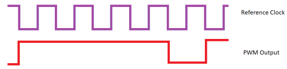
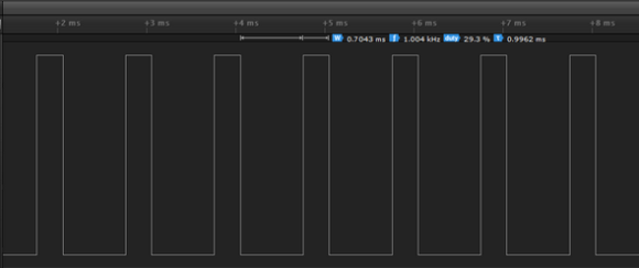
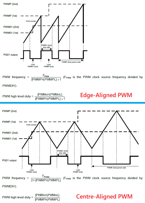
The basic theme of PWM generation as with any microcontroller is to change the logic state of an output pin when the count in it associated TACCR register matches with the count in its timer’s counter register – simply like a binary comparator. This process is called compare-match process. This is exactly the same idea used in MSP430s. Check the rudimentary timing diagram below. For five successive falling edges of the reference clock, the PWM output is high and for one edge, the output is low, resulting in about 83% duty cycle. The reference clock here is actually the timer clock and the comparison is done by comparing the count stored in TACCRn. Varying TACCRn’s count results in duty cycle change.
![PWM]()
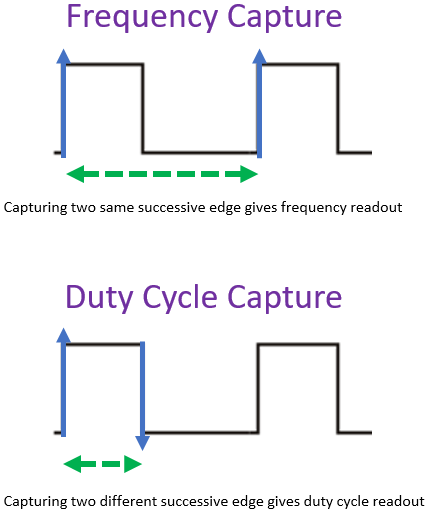
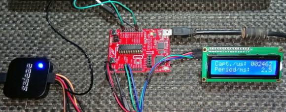
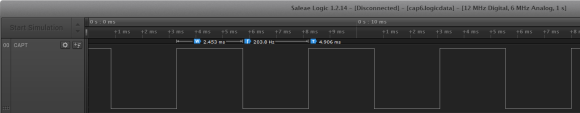
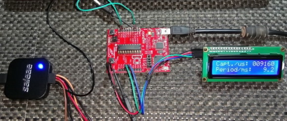
Input capture is somewhat just the opposite of PWM generation. In capture mode, CC channels can be used to record time-related info of an incoming waveform. A timer in this mode can be left to run on its own. When a waveform edge is detected, the corresponding time count of the timer is stored in CC register. With two such consecutive captures, we get a difference in timer’s time counts. This difference can be used to measure frequency if the captured events are alike (two successive rising/falling edges) or duty cycle if the captured events are different (different edges). Again, TACCRn stores the time capture when a capture event occurs.
![Capture_modes]()
As an example, check the arbitrary timing diagram below:
![Capture Mode]()
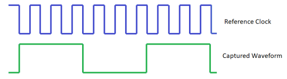
Here four falling edges of reference clock (timer clock) is equal to the high or on time of the captured waveform. Since the reference clock’s period is known, we can deduce pulse width.
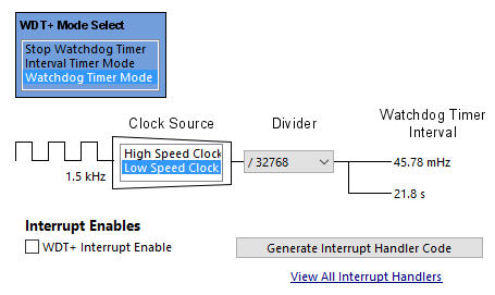
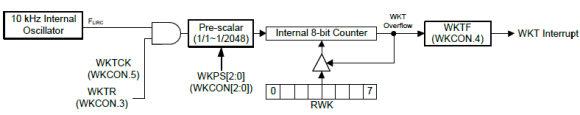
WDT+
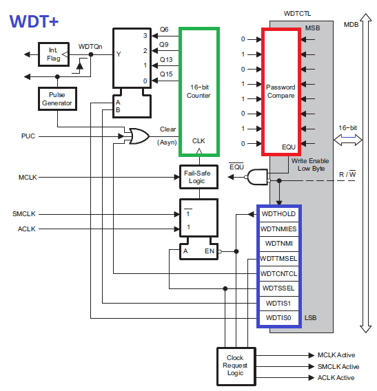
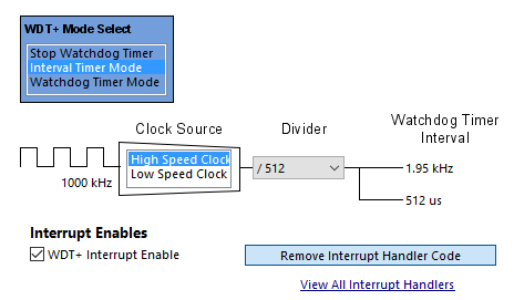
WDT+ is a 15/16-bit watchdog timer. It is mainly intended to prevent unanticipated loops or stuck up conditions due to malfunctions or firmware bugs. The concept behind any watchdog timer is to regularly refresh a counter so that the count never reaches a predefined limit. If due to any reason this limit is exceeded, a reset is issued, causing the host micro to start over again.
![WDT+ Block Diagram]()
WDT+ can additional be used as an interval timer just like other timers if watchdog timer functionality is not needed. We can, then, use WDT+ for time-base generations.
WDT+ is password protected and so a wrong password causes it to fail and reset immediately. This is the red box in the diagram above. Whenever we need to change anything related to WDT+, we have to enter the correct password which is 0x5A00. WDT+ consists of a 16-bit counter (green box) but we don’t have access to it. The purple region consists of WDT options. The red and the purple boxes make up Watchdog Control (WDTCTL) register and this is what we are only allowed to code.
Free Running Timer
Free running timers are useful in many cases. Free running timers can be used as random number generators, time delay generators, instance markers, etc. Consider the case of time delay generation for instance. Rather than using wasteful CPU-cycle dependent software delay loops, it is much wiser to use a hardware timer to create precise delays and timed events. In terms of ideal coding, no task should keep CPU busy unnecessarily nor should it keep other tasks waiting for its completion. Best coding and design are achieved if things are arranged in such an orderly way that that there is almost no wastage of any resource at all.
![Free Running Timer]()
By free-running what I really mean is we start a timer at the beginning of our code and keep it running without timer interrupt. We just take note of its counter. Here we will see how to use Timer_A3 like a free running timer and we will use it to blink Launchpad board’s LEDs.
Code Example
#include <msp430.h>
void GPIO_graceInit(void);
void BCSplus_graceInit(void);
void Timer0_A3_graceInit(void);
void System_graceInit(void);
void WDTplus_graceInit(void);
#pragma vector=TIMER0_A1_VECTOR
__interrupt void TIMER0_A1_ISR_HOOK(void)
{
}
void main(void)
{
/* Stop watchdog timer from timing out during initial start-up. */
WDTCTL = WDTPW | WDTHOLD;
/* initialize Config for the MSP430 GPIO */
GPIO_graceInit();
/* initialize Config for the MSP430 2xx family clock systems (BCS) */
BCSplus_graceInit();
/* initialize Config for the MSP430 A3 Timer0 */
Timer0_A3_graceInit();
/* initialize Config for the MSP430 System Registers */
System_graceInit();
/* initialize Config for the MSP430 WDT+ */
WDTplus_graceInit();
while(1)
{
if(TA0R >= 32768)
{
P1OUT |= BIT6;
P1OUT &= ~BIT0;
}
else
{
P1OUT |= BIT0;
P1OUT &= ~BIT6;
}
};
}
void BCSplus_graceInit(void)
{
/* USER CODE START (section: BCSplus_graceInit_prologue) */
/* User initialization code */
/* USER CODE END (section: BCSplus_graceInit_prologue) */
/*
* Basic Clock System Control 2
*
* SELM_0 -- DCOCLK
* DIVM_0 -- Divide by 1
* ~SELS -- DCOCLK
* DIVS_0 -- Divide by 1
* ~DCOR -- DCO uses internal resistor
*
* Note: ~<BIT> indicates that <BIT> has value zero
*/
BCSCTL2 = SELM_0 | DIVM_0 | DIVS_0;
if (CALBC1_1MHZ != 0xFF) {
/* Follow recommended flow. First, clear all DCOx and MODx bits. Then
* apply new RSELx values. Finally, apply new DCOx and MODx bit values.
*/
DCOCTL = 0x00;
BCSCTL1 = CALBC1_1MHZ; /* Set DCO to 1MHz */
DCOCTL = CALDCO_1MHZ;
}
/*
* Basic Clock System Control 1
*
* XT2OFF -- Disable XT2CLK
* ~XTS -- Low Frequency
* DIVA_0 -- Divide by 1
*
* Note: ~XTS indicates that XTS has value zero
*/
BCSCTL1 |= XT2OFF | DIVA_0;
/*
* Basic Clock System Control 3
*
* XT2S_0 -- 0.4 - 1 MHz
* LFXT1S_0 -- If XTS = 0, XT1 = 32768kHz Crystal ; If XTS = 1, XT1 = 0.4 - 1-MHz crystal or resonator
* XCAP_1 -- ~6 pF
*/
BCSCTL3 = XT2S_0 | LFXT1S_0 | XCAP_1;
/* USER CODE START (section: BCSplus_graceInit_epilogue) */
/* User code */
/* USER CODE END (section: BCSplus_graceInit_epilogue) */
}
void GPIO_graceInit(void)
{
/* USER CODE START (section: GPIO_graceInit_prologue) */
/* User initialization code */
/* USER CODE END (section: GPIO_graceInit_prologue) */
/* Port 1 Output Register */
P1OUT = 0;
/* Port 1 Direction Register */
P1DIR = BIT0 | BIT6;
/* Port 1 Interrupt Edge Select Register */
P1IES = 0;
/* Port 1 Interrupt Flag Register */
P1IFG = 0;
/* Port 2 Output Register */
P2OUT = 0;
/* Port 2 Port Select Register */
P2SEL &= ~(BIT6 | BIT7);
/* Port 2 Direction Register */
P2DIR = 0;
/* Port 2 Interrupt Edge Select Register */
P2IES = 0;
/* Port 2 Interrupt Flag Register */
P2IFG = 0;
/* USER CODE START (section: GPIO_graceInit_epilogue) */
/* User code */
/* USER CODE END (section: GPIO_graceInit_epilogue) */
}
void Timer0_A3_graceInit(void)
{
/* USER CODE START (section: Timer0_A3_graceInit_prologue) */
/* User initialization code */
/* USER CODE END (section: Timer0_A3_graceInit_prologue) */
/*
* TA0CTL, Timer_A3 Control Register
*
* TASSEL_2 -- SMCLK
* ID_3 -- Divider - /8
* MC_2 -- Continuous Mode
*/
TA0CTL = TASSEL_2 | ID_3 | MC_2;
/* USER CODE START (section: Timer0_A3_graceInit_epilogue) */
/* User code */
/* USER CODE END (section: Timer0_A3_graceInit_epilogue) */
}
void System_graceInit(void)
{
/* USER CODE START (section: System_graceInit_prologue) */
/* User initialization code */
/* USER CODE END (section: System_graceInit_prologue) */
/*
* SR, Status Register
*
* ~SCG1 -- Disable System clock generator 1
* ~SCG0 -- Disable System clock generator 0
* ~OSCOFF -- Oscillator On
* ~CPUOFF -- CPU On
* GIE -- General interrupt enable
*
* Note: ~<BIT> indicates that <BIT> has value zero
*/
__bis_SR_register(GIE);
/* USER CODE START (section: System_graceInit_epilogue) */
/* User code */
/* USER CODE END (section: System_graceInit_epilogue) */
}
void WDTplus_graceInit(void)
{
/* USER CODE START (section: RTC_B_graceInit_prologue) */
/* User initialization code */
/* USER CODE END (section: RTC_B_graceInit_prologue) */
/*
* WDTCTL, Watchdog Timer+ Register
*
* WDTPW -- Watchdog password
* WDTHOLD -- Watchdog timer+ is stopped
* ~WDTNMIES -- NMI on rising edge
* ~WDTNMI -- Reset function
* ~WDTTMSEL -- Watchdog mode
* ~WDTCNTCL -- No action
* ~WDTSSEL -- SMCLK
* ~WDTIS0 -- Watchdog clock source bit0 disabled
* ~WDTIS1 -- Watchdog clock source bit1 disabled
*
* Note: ~<BIT> indicates that <BIT> has value zero
*/
WDTCTL = WDTPW | WDTHOLD;
/* USER CODE START (section: RTC_B_graceInit_epilogue) */
/* User code */
/* USER CODE END (section: RTC_B_graceInit_epilogue) */
}
Simulation
![Free Running Timer Simulation]()
Explanation
In this demo, Timer_A3 is clocked with SMCLK divided by 8. SMCLK has a frequency of 1MHz and so Timer_A3 is feed with a 125kHz clock. This gives us a timer tick period of 8 microseconds. Since the timer is programmed to operate in continuous mode, i.e. it will count from 0 to top value of 65535, the timer will overflow roughly about every 500 milliseconds. We, thus, have an interval window of 500 milliseconds.
![Grace Free Running Timer Settings]()
/*
* TA0CTL, Timer_A3 Control Register
*
* TASSEL_2 -- SMCLK
* ID_3 -- Divider - /8
* MC_2 -- Continuous Mode
*/
TA0CTL = TASSEL_2 | ID_3 | MC_2;
We want to blink the Launchpad board’s LEDs at the rate of 250 milliseconds. Thus, we need to check or compare if the counter register TA0R has gone past 50% of the full scale 16-bit value. This is an event marker because with reference to this mark, we toggle the states of the LEDs. The idea shown here is actually the concept with which PWMs are generated by compare-match principle inside timer hardware and so it is worth understanding this idea.
if(TA0R >= 32768)
{
P1OUT |= BIT6;
P1OUT &= ~BIT0;
}
else
{
P1OUT |= BIT0;
P1OUT &= ~BIT6;
}
Demo
![Free Running Timer]()
![Free Running Timer (1)]()
![Free Running Timer (2)]()
Demo video: https://www.youtube.com/watch?v=OGvswRhb7ds.
Timer Interrupt
We have already seen how to use a timer as a free-running timer. However, in most cases we will need timer interrupts. Timer interrupts are periodic interrupts which means they occur at fixed intervals just like clock ticks. Owing to this nature we can split multiple tasks and make them appear as if all of them are happening concurrently. For instance, we can use an ADC to measure the temperature of a room while using a timer to periodically update the temperature display. This is the main concept in driving segment displays, dot-matrix displays and many more although it is not the only thing we can do with timer interrupts.
![serial-7-seg-display-2-board-large_default-12x]()
A timer interrupt is also at the heart of any typical Real-Time Operating System (RTOS).
![Basic RTOS Concept]()
Here we will stick to a simple example of a seven-segment display-based second counter. Rather than demoing LED blinking with timer interrupt I chose this example because this has many applications in the field of displaying information on LED-based displays. The same concept can be expanded for dot-matrix displays, LED bar graphs, alphanumerical segmented displays and many more.
Code Example
#include <msp430.h>
unsigned int ms = 0;
unsigned int value = 0;
unsigned char n = 0;
unsigned char seg = 0;
const unsigned char num[10] = {0xC0, 0xF9, 0xA4, 0xB0, 0x99, 0x92, 0x82, 0xF8, 0x80, 0x90};
void GPIO_graceInit(void);
void BCSplus_graceInit(void);
void Timer0_A3_graceInit(void);
void System_graceInit(void);
void WDTplus_graceInit(void);
#pragma vector=TIMER0_A1_VECTOR
__interrupt void TIMER0_A1_ISR_HOOK(void)
{
ms++;
if(ms > 999)
{
ms = 0;
value++;
if(value > 9999)
{
value = 0;
}
}
switch(seg)
{
case 1:
{
n = (value / 1000);
P2OUT = num[n];
P1OUT = 0xE0;
break;
}
case 2:
{
n = ((value / 100) % 10);
P2OUT = num[n];
P1OUT = 0xD0;
break;
}
case 3:
{
n = ((value / 10) % 10);
P2OUT = num[n];
P1OUT = 0xB0;
break;
}
case 4:
{
n = (value % 10);
P2OUT = num[n];
P1OUT = 0x70;
break;
}
}
seg++;
if(seg > 4)
{
seg = 1;
}
TA0CTL &= ~TAIFG;
TAIV &= ~TA0IV_TAIFG;
}
void main(void)
{
GPIO_graceInit();
/* initialize Config for the MSP430 2xx family clock systems (BCS) */
BCSplus_graceInit();
/* initialize Config for the MSP430 A3 Timer0 */
Timer0_A3_graceInit();
/* initialize Config for the MSP430 System Registers */
System_graceInit();
/* initialize Config for the MSP430 WDT+ */
WDTplus_graceInit();
while(1)
{
};
}
void GPIO_graceInit(void)
{
/* USER CODE START (section: GPIO_graceInit_prologue) */
/* User initialization code */
/* USER CODE END (section: GPIO_graceInit_prologue) */
/* Port 1 Output Register */
P1OUT = 0;
/* Port 1 Direction Register */
P1DIR = BIT4 | BIT5 | BIT6 | BIT7;
/* Port 1 Interrupt Edge Select Register */
P1IES = 0;
/* Port 1 Interrupt Flag Register */
P1IFG = 0;
/* Port 2 Output Register */
P2OUT = 0;
/* Port 2 Port Select Register */
P2SEL &= ~(BIT6 | BIT7);
/* Port 2 Direction Register */
P2DIR = BIT0 | BIT1 | BIT2 | BIT3 | BIT4 | BIT5 | BIT6 | BIT7;
/* Port 2 Interrupt Edge Select Register */
P2IES = 0;
/* Port 2 Interrupt Flag Register */
P2IFG = 0;
/* USER CODE START (section: GPIO_graceInit_epilogue) */
/* User code */
/* USER CODE END (section: GPIO_graceInit_epilogue) */
}
void BCSplus_graceInit(void)
{
/* USER CODE START (section: BCSplus_graceInit_prologue) */
/* User initialization code */
/* USER CODE END (section: BCSplus_graceInit_prologue) */
/*
* Basic Clock System Control 2
*
* SELM_0 -- DCOCLK
* DIVM_0 -- Divide by 1
* ~SELS -- DCOCLK
* DIVS_0 -- Divide by 1
* ~DCOR -- DCO uses internal resistor
*
* Note: ~<BIT> indicates that <BIT> has value zero
*/
BCSCTL2 = SELM_0 | DIVM_0 | DIVS_0;
if (CALBC1_1MHZ != 0xFF) {
/* Follow recommended flow. First, clear all DCOx and MODx bits. Then
* apply new RSELx values. Finally, apply new DCOx and MODx bit values.
*/
DCOCTL = 0x00;
BCSCTL1 = CALBC1_1MHZ; /* Set DCO to 1MHz */
DCOCTL = CALDCO_1MHZ;
}
/*
* Basic Clock System Control 1
*
* XT2OFF -- Disable XT2CLK
* ~XTS -- Low Frequency
* DIVA_0 -- Divide by 1
*
* Note: ~XTS indicates that XTS has value zero
*/
BCSCTL1 |= XT2OFF | DIVA_0;
/*
* Basic Clock System Control 3
*
* XT2S_0 -- 0.4 - 1 MHz
* LFXT1S_0 -- If XTS = 0, XT1 = 32768kHz Crystal ; If XTS = 1, XT1 = 0.4 - 1-MHz crystal or resonator
* XCAP_1 -- ~6 pF
*/
BCSCTL3 = XT2S_0 | LFXT1S_0 | XCAP_1;
/* USER CODE START (section: BCSplus_graceInit_epilogue) */
/* User code */
/* USER CODE END (section: BCSplus_graceInit_epilogue) */
}
void Timer0_A3_graceInit(void)
{
/* USER CODE START (section: Timer0_A3_graceInit_prologue) */
/* User initialization code */
/* USER CODE END (section: Timer0_A3_graceInit_prologue) */
/* TA0CCR0, Timer_A Capture/Compare Register 0 */
TA0CCR0 = 999;
/*
* TA0CTL, Timer_A3 Control Register
*
* TASSEL_2 -- SMCLK
* ID_0 -- Divider - /1
* MC_1 -- Up Mode
*/
TA0CTL = TASSEL_2 | ID_0 | MC_1 | TAIE;
/* USER CODE START (section: Timer0_A3_graceInit_epilogue) */
/* User code */
/* USER CODE END (section: Timer0_A3_graceInit_epilogue) */
}
void System_graceInit(void)
{
/* USER CODE START (section: System_graceInit_prologue) */
/* User initialization code */
/* USER CODE END (section: System_graceInit_prologue) */
/*
* SR, Status Register
*
* ~SCG1 -- Disable System clock generator 1
* ~SCG0 -- Disable System clock generator 0
* ~OSCOFF -- Oscillator On
* ~CPUOFF -- CPU On
* GIE -- General interrupt enable
*
* Note: ~<BIT> indicates that <BIT> has value zero
*/
__bis_SR_register(GIE);
/* USER CODE START (section: System_graceInit_epilogue) */
/* User code */
/* USER CODE END (section: System_graceInit_epilogue) */
}
void WDTplus_graceInit(void)
{
/* USER CODE START (section: RTC_B_graceInit_prologue) */
/* User initialization code */
/* USER CODE END (section: RTC_B_graceInit_prologue) */
/*
* WDTCTL, Watchdog Timer+ Register
*
* WDTPW -- Watchdog password
* WDTHOLD -- Watchdog timer+ is stopped
* ~WDTNMIES -- NMI on rising edge
* ~WDTNMI -- Reset function
* ~WDTTMSEL -- Watchdog mode
* ~WDTCNTCL -- No action
* ~WDTSSEL -- SMCLK
* ~WDTIS0 -- Watchdog clock source bit0 disabled
* ~WDTIS1 -- Watchdog clock source bit1 disabled
*
* Note: ~<BIT> indicates that <BIT> has value zero
*/
WDTCTL = WDTPW | WDTHOLD;
/* USER CODE START (section: RTC_B_graceInit_epilogue) */
/* User code */
/* USER CODE END (section: RTC_B_graceInit_epilogue) */
}
Simulation
![Timer Interrupt Simulation]()
Explanation
In this demo, Timer_A3 is configured as an up counting timer, i.e. it will count from 0 to a top value determined by the contents of TA0CCR0 register. Again, SMCLK is used as the clock source for the timer but this time it is not scaled down. SMCLK is set to 1 MHz and so does Timer_A3. This means every one tick of Timer_A3 is one microsecond in duration. To make it appear that all four seven segments are simultaneously on without any flickering, we need to scan them fast enough to fool our eyes. We also have to ensure that each segment gets enough time to light up properly. In order to do so we need to scan the segments at one millisecond rate. To get one millisecond from a timer with one microsecond tick interval, we have to load it with 999, not 1000. This is so because from 0 to 999 the total number of ticks is 1000. In short, 1000 times 1 microsecond equals 1 millisecond. Thus, TA0CCR0 is loaded with 999.
![Grace Settings for Timer Interrupt]()
/* TA0CCR0, Timer_A Capture/Compare Register 0 */
TA0CCR0 = 999;
/*
* TA0CTL, Timer_A3 Control Register
*
* TASSEL_2 -- SMCLK
* ID_0 -- Divider - /1
* MC_1 -- Up Mode
*/
TA0CTL = TASSEL_2 | ID_0 | MC_1 | TAIE;
Everything else in this demo is done inside Timer_A3 interrupt subroutine (ISR). There are two parts inside the ISR. The first as shown below is responsible for counting time.
ms++;
if(ms > 999)
{
ms = 0;
value++;
if(value > 9999)
{
value = 0;
}
}
The other portion is tasked with the LED segment scanning and data display part. At every millisecond, a new segment is turned on, keeping others off. At the end of the ISR, interrupt flags are cleared.
switch(seg)
{
case 1:
{
n = (value / 1000);
P2OUT = num[n];
P1OUT = 0xE0;
break;
}
case 2:
{
n = ((value / 100) % 10);
P2OUT = num[n];
P1OUT = 0xD0;
break;
}
case 3:
{
n = ((value / 10) % 10);
P2OUT = num[n];
P1OUT = 0xB0;
break;
}
case 4:
{
n = (value % 10);
P2OUT = num[n];
P1OUT = 0x70;
break;
}
}
seg++;
if(seg > 4)
{
seg = 1;
}
TA0CTL &= ~TAIFG;
TAIV &= ~TA0IV_TAIFG;
Demo
![Timer Interrupt Demo]()
Demo video: https://www.youtube.com/watch?v=8EG9rcOAATo.
Pulse Width Modulation (PWM)
At present PWM hardware is a must for any microcontroller because in many cases, it is needed to extract something more than ones and zeros from it. For example, consider the case of a sine wave generator. Without the aid of a Digital-to-Analog Converter (DAC), generating sine waves seems nearly impossible. However, we can still achieve that using Pulse Width Modulation (PWM) and some mathematical tricks.
![PWM Sine Generation]()
Generating waveforms, pulses with variable widths, patterns, sounds, communications pulses like those in IR remotes, speed control, etc require PWM hardware. Keep in mind that all MSP30x2xxx devices do not have any inbuilt DAC and so if analogue output is needed, we can use PWM with necessary external RC filtering to create analogue output.
A few things must be observed before using MSP430 PWM hardware:
- Timer A PWMs are general purpose PWMs.
- There’s no separate option for dead-time.
- Maximum PWM resolution is 16-bit.
- CC Channel 0 is not like the other two channels. It has limited output options and in GRACE you’ll notice that you can’t set PWM duty cycle.
- PWM frequency and resolution are interdependent.
- PWM pins are limitedly remappable.
Code Example
#include <msp430.h>
#include "delay.h"
void GPIO_graceInit(void);
void BCSplus_graceInit(void);
void Timer0_A3_graceInit(void);
void System_graceInit(void);
void WDTplus_graceInit(void);
void main(void)
{
unsigned int pwm_value = 0;
/* Stop watchdog timer from timing out during initial start-up. */
WDTCTL = WDTPW | WDTHOLD;
/* initialize Config for the MSP430 GPIO */
GPIO_graceInit();
/* initialize Config for the MSP430 2xx family clock systems (BCS) */
BCSplus_graceInit();
/* initialize Config for the MSP430 A3 Timer0 */
Timer0_A3_graceInit();
/* initialize Config for the MSP430 System Registers */
System_graceInit();
/* initialize Config for the MSP430 WDT+ */
WDTplus_graceInit();
while(1)
{
for(pwm_value = 0; pwm_value < 1000; pwm_value++)
{
TA0CCR1 = pwm_value;
TA0CCR2 = pwm_value;
delay_ms(1);
}
for(pwm_value = 999; pwm_value > 0; pwm_value--)
{
TA0CCR1 = pwm_value;
TA0CCR2 = pwm_value;
delay_ms(1);
}
};
}
void GPIO_graceInit(void)
{
/* USER CODE START (section: GPIO_graceInit_prologue) */
/* User initialization code */
/* USER CODE END (section: GPIO_graceInit_prologue) */
/* Port 1 Port Select 2 Register */
P1SEL2 = BIT4;
/* Port 1 Output Register */
P1OUT = 0;
/* Port 1 Port Select Register */
P1SEL = BIT1 | BIT4 | BIT6;
/* Port 1 Direction Register */
P1DIR = BIT1 | BIT4 | BIT6;
/* Port 1 Interrupt Edge Select Register */
P1IES = 0;
/* Port 1 Interrupt Flag Register */
P1IFG = 0;
/* Port 2 Output Register */
P2OUT = 0;
/* Port 2 Port Select Register */
P2SEL &= ~(BIT6 | BIT7);
/* Port 2 Direction Register */
P2DIR = 0;
/* Port 2 Interrupt Edge Select Register */
P2IES = 0;
/* Port 2 Interrupt Flag Register */
P2IFG = 0;
/* USER CODE START (section: GPIO_graceInit_epilogue) */
/* User code */
/* USER CODE END (section: GPIO_graceInit_epilogue) */
}
void BCSplus_graceInit(void)
{
/* USER CODE START (section: BCSplus_graceInit_prologue) */
/* User initialization code */
/* USER CODE END (section: BCSplus_graceInit_prologue) */
/*
* Basic Clock System Control 2
*
* SELM_0 -- DCOCLK
* DIVM_0 -- Divide by 1
* ~SELS -- DCOCLK
* DIVS_0 -- Divide by 1
* ~DCOR -- DCO uses internal resistor
*
* Note: ~<BIT> indicates that <BIT> has value zero
*/
BCSCTL2 = SELM_0 | DIVM_0 | DIVS_0;
if (CALBC1_1MHZ != 0xFF) {
/* Follow recommended flow. First, clear all DCOx and MODx bits. Then
* apply new RSELx values. Finally, apply new DCOx and MODx bit values.
*/
DCOCTL = 0x00;
BCSCTL1 = CALBC1_1MHZ; /* Set DCO to 1MHz */
DCOCTL = CALDCO_1MHZ;
}
/*
* Basic Clock System Control 1
*
* XT2OFF -- Disable XT2CLK
* ~XTS -- Low Frequency
* DIVA_0 -- Divide by 1
*
* Note: ~XTS indicates that XTS has value zero
*/
BCSCTL1 |= XT2OFF | DIVA_0;
/*
* Basic Clock System Control 3
*
* XT2S_0 -- 0.4 - 1 MHz
* LFXT1S_2 -- If XTS = 0, XT1 = VLOCLK ; If XTS = 1, XT1 = 3 - 16-MHz crystal or resonator
* XCAP_1 -- ~6 pF
*/
BCSCTL3 = XT2S_0 | LFXT1S_2 | XCAP_1;
/* USER CODE START (section: BCSplus_graceInit_epilogue) */
/* User code */
/* USER CODE END (section: BCSplus_graceInit_epilogue) */
}
void Timer0_A3_graceInit(void)
{
/* USER CODE START (section: Timer0_A3_graceInit_prologue) */
/* User initialization code */
/* USER CODE END (section: Timer0_A3_graceInit_prologue) */
/*
* TA0CCTL0, Capture/Compare Control Register 0
*
* CM_0 -- No Capture
* CCIS_0 -- CCIxA
* ~SCS -- Asynchronous Capture
* ~SCCI -- Latched capture signal (read)
* ~CAP -- Compare mode
* OUTMOD_4 -- PWM output mode: 4 - Toggle
*
* Note: ~<BIT> indicates that <BIT> has value zero
*/
TA0CCTL0 = CM_0 | CCIS_0 | OUTMOD_4;
/*
* TA0CCTL1, Capture/Compare Control Register 1
*
* CM_0 -- No Capture
* CCIS_0 -- CCIxA
* ~SCS -- Asynchronous Capture
* ~SCCI -- Latched capture signal (read)
* ~CAP -- Compare mode
* OUTMOD_3 -- PWM output mode: 3 - PWM set/reset
*
* Note: ~<BIT> indicates that <BIT> has value zero
*/
TA0CCTL1 = CM_0 | CCIS_0 | OUTMOD_3;
/*
* TA0CCTL2, Capture/Compare Control Register 2
*
* CM_0 -- No Capture
* CCIS_0 -- CCIxA
* ~SCS -- Asynchronous Capture
* ~SCCI -- Latched capture signal (read)
* ~CAP -- Compare mode
* OUTMOD_7 -- PWM output mode: 7 - PWM reset/set
*
* Note: ~<BIT> indicates that <BIT> has value zero
*/
TA0CCTL2 = CM_0 | CCIS_0 | OUTMOD_7;
/* TA0CCR0, Timer_A Capture/Compare Register 0 */
TA0CCR0 = 999;
/* TA0CCR1, Timer_A Capture/Compare Register 1 */
TA0CCR1 = 10;
/* TA0CCR2, Timer_A Capture/Compare Register 2 */
TA0CCR2 = 10;
/*
* TA0CTL, Timer_A3 Control Register
*
* TASSEL_2 -- SMCLK
* ID_0 -- Divider - /1
* MC_1 -- Up Mode
*/
TA0CTL = TASSEL_2 | ID_0 | MC_1;
/* USER CODE START (section: Timer0_A3_graceInit_epilogue) */
/* User code */
/* USER CODE END (section: Timer0_A3_graceInit_epilogue) */
}
void System_graceInit(void)
{
/* USER CODE START (section: System_graceInit_prologue) */
/* User initialization code */
/* USER CODE END (section: System_graceInit_prologue) */
/* Clear oscillator fault flag with software delay */
do
{
// Clear OSC fault flag
IFG1 &= ~OFIFG;
// 50us delay
__delay_cycles(50);
} while (IFG1 & OFIFG);
/*
* SR, Status Register
*
* ~SCG1 -- Disable System clock generator 1
* ~SCG0 -- Disable System clock generator 0
* ~OSCOFF -- Oscillator On
* ~CPUOFF -- CPU On
* GIE -- General interrupt enable
*
* Note: ~<BIT> indicates that <BIT> has value zero
*/
__bis_SR_register(GIE);
/* USER CODE START (section: System_graceInit_epilogue) */
/* User code */
/* USER CODE END (section: System_graceInit_epilogue) */
}
void WDTplus_graceInit(void)
{
/* USER CODE START (section: RTC_B_graceInit_prologue) */
/* User initialization code */
/* USER CODE END (section: RTC_B_graceInit_prologue) */
/*
* WDTCTL, Watchdog Timer+ Register
*
* WDTPW -- Watchdog password
* WDTHOLD -- Watchdog timer+ is stopped
* ~WDTNMIES -- NMI on rising edge
* ~WDTNMI -- Reset function
* ~WDTTMSEL -- Watchdog mode
* ~WDTCNTCL -- No action
* ~WDTSSEL -- SMCLK
* ~WDTIS0 -- Watchdog clock source bit0 disabled
* ~WDTIS1 -- Watchdog clock source bit1 disabled
*
* Note: ~<BIT> indicates that <BIT> has value zero
*/
WDTCTL = WDTPW | WDTHOLD;
/* USER CODE START (section: RTC_B_graceInit_epilogue) */
/* User code */
/* USER CODE END (section: RTC_B_graceInit_epilogue) */
}
Simulation
![PWM Simulation]()
Explanation
Just as in the previous example, SMCLK is set to 1 MHz. Timer_A3 is also setup for up counting with a top value of 999, resulting in 1ms time duration. Note no interrupt is used and other CCR registers are loaded with 10 – an arbitrary value.
/* TA0CCR0, Timer_A Capture/Compare Register 0 */
TA0CCR0 = 999;
/* TA0CCR1, Timer_A Capture/Compare Register 1 */
TA0CCR1 = 10;
/* TA0CCR2, Timer_A Capture/Compare Register 2 */
TA0CCR2 = 10;
/*
* TA0CTL, Timer_A3 Control Register
*
* TASSEL_2 -- SMCLK
* ID_0 -- Divider - /1
* MC_1 -- Up Mode
*/
TA0CTL = TASSEL_2 | ID_0 | MC_1;
Prior to Timer_A3 setup, CC channels are setup. OUTMOD is that stuff that sets PWM type.
/*
* TA0CCTL0, Capture/Compare Control Register 0
*
* CM_0 -- No Capture
* CCIS_0 -- CCIxA
* ~SCS -- Asynchronous Capture
* ~SCCI -- Latched capture signal (read)
* ~CAP -- Compare mode
* OUTMOD_4 -- PWM output mode: 4 - Toggle
*
* Note: ~<BIT> indicates that <BIT> has value zero
*/
TA0CCTL0 = CM_0 | CCIS_0 | OUTMOD_4;
/*
* TA0CCTL1, Capture/Compare Control Register 1
*
* CM_0 -- No Capture
* CCIS_0 -- CCIxA
* ~SCS -- Asynchronous Capture
* ~SCCI -- Latched capture signal (read)
* ~CAP -- Compare mode
* OUTMOD_3 -- PWM output mode: 3 - PWM set/reset
*
* Note: ~<BIT> indicates that <BIT> has value zero
*/
TA0CCTL1 = CM_0 | CCIS_0 | OUTMOD_3;
/*
* TA0CCTL2, Capture/Compare Control Register 2
*
* CM_0 -- No Capture
* CCIS_0 -- CCIxA
* ~SCS -- Asynchronous Capture
* ~SCCI -- Latched capture signal (read)
* ~CAP -- Compare mode
* OUTMOD_7 -- PWM output mode: 7 - PWM reset/set
*
* Note: ~<BIT> indicates that <BIT> has value zero
*/
TA0CCTL2 = CM_0 | CCIS_0 | OUTMOD_7;
In this demo, three different PWMs are set to show the differences.
![Grace PWM1]()
![Grace PWM2]()
![Grace PWM3]()
PWMs can be of the following types:
![PWM Modes]()
Note that CCR0 has limited PWM options and it is the value of its register that sets PWM frequency. The other CCR registers are loaded with values that determine respective PWM duty cycles.
Demo
![PWM Demo 1]()
![PWM Capture Demo 1]()
![PWM Demo 2]()
![PWM Capture Demo 2]()
Demo video: https://www.youtube.com/watch?v=dbSPi6LbsQg.
Timer Input Capture
In many cases, it is needed to measure the timing info like period, frequency, duty cycle, etc of an incoming signal. Based on these data we can find out the RPM of a robot’s wheel, the pulse widths of an IR remote stream carrying command information, the frequency of AC mains, the patterns of an incoming waveform, etc. Hence comes the purpose of timer input captures.
![Capture]()
We know that Timer A3 has three such CC channels and so there are three capture inputs per Timer A module. We can use these channels to capture incoming waveforms of unknown frequencies/duty cycles and have them measured with respect to a known clock like SMCLK.
Again a few things must be observed before using MSP430 input capture hardware:
- Signals coming to input pins must never cross the max. VDD limit or fall below ground level (i.e. sensing negative potentials).
- It is better to galvanically isolate input pins if they are to sense external high voltage signals.
- Input pins must not be left floating.
- Unless needed, it is wise not to use RC filters for inputs.
- Input capture pins are limited remappable just like PWM pins.
- Timer clock must be set as such that we get maximum measurement resolution without compromising reliability.
- Timer overruns/overflows must be taken into account.
- Timer capture inputs can be tied to power pins internally and connecting so results in no measurements. When not capturing anything, select stop mode and clear the timer.
Code Example
#include <msp430.h>
#include "delay.h"
#include "lcd.h"
unsigned int overflow_count = 0;
unsigned int pulse_ticks = 0;
unsigned int start_time = 0;
unsigned int end_time = 0;
void GPIO_graceInit(void);
void BCSplus_graceInit(void);
void Timer0_A3_graceInit(void);
void Timer1_A3_graceInit(void);
void System_graceInit(void);
void WDTplus_graceInit(void);
void lcd_print(unsigned char x_pos, unsigned char y_pos, unsigned long value);
#pragma vector=TIMER1_A1_VECTOR
__interrupt void TIMER1_A1_ISR_HOOK(void)
{
if(TA1IV == TA1IV_TACCR1)
{
end_time = TA1CCR1;
pulse_ticks = (end_time - start_time);
start_time = end_time;
TA1CCTL1 &= ~CCIFG;
}
}
void main(void)
{
unsigned char i = 0;
unsigned long time_period = 0;
/* Stop watchdog timer from timing out during initial start-up. */
WDTCTL = WDTPW | WDTHOLD;
/* initialize Config for the MSP430 GPIO */
GPIO_graceInit();
/* initialize Config for the MSP430 2xx family clock systems (BCS) */
BCSplus_graceInit();
/* initialize Config for the MSP430 A3 Timer0 */
Timer0_A3_graceInit();
/* initialize Config for the MSP430 A3 Timer0 */
Timer1_A3_graceInit();
/* initialize Config for the MSP430 System Registers */
System_graceInit();
/* initialize Config for the MSP430 WDT+ */
WDTplus_graceInit();
LCD_init();
LCD_clear_home();
LCD_goto(0, 0);
LCD_putstr("Capt./us:");
delay_ms(10);
while(1)
{
if((P1IN & BIT3) == 0)
{
P1OUT |= BIT0;
while((P1IN & BIT3) == 0);
i++;
if(i > 9)
{
i = 0;
}
P1OUT &= ~BIT0;
}
switch(i)
{
case 1:
{
TA0CCR0 = 9999;
LCD_goto(0, 1);
LCD_putstr("Period/ms: 20");
break;
}
case 2:
{
TA0CCR0 = 4999;
LCD_goto(0, 1);
LCD_putstr("Period/ms: 10");
break;
}
case 3:
{
TA0CCR0 = 1999;
LCD_goto(0, 1);
LCD_putstr("Period/ms: 4");
break;
}
case 4:
{
TA0CCR0 = 999;
LCD_goto(0, 1);
LCD_putstr("Period/ms: 2");
break;
}
case 5:
{
TA0CCR0 = 166;
LCD_goto(0, 1);
LCD_putstr("Period/us: 334");
break;
}
case 6:
{
TA0CCR0 = 1230;
LCD_goto(0, 1);
LCD_putstr("Period/ms: 2.5");
break;
}
case 7:
{
TA0CCR0 = 2626;
LCD_goto(0, 1);
LCD_putstr("Period/ms: 5.3");
break;
}
case 8:
{
TA0CCR0 = 4579;
LCD_goto(0, 1);
LCD_putstr("Period/ms: 9.2");
break;
}
case 9:
{
TA0CCR0 = 499;
LCD_goto(0, 1);
LCD_putstr("Period/ms: 1");
break;
}
default:
{
TA0CCR0 = 6964;
LCD_goto(0, 1);
LCD_putstr("Period/ms: 13.9");
break;
}
}
time_period = (pulse_ticks >> 1);
lcd_print(10, 0, time_period);
delay_ms(400);
};
}
void GPIO_graceInit(void)
{
/* USER CODE START (section: GPIO_graceInit_prologue) */
/* User initialization code */
/* USER CODE END (section: GPIO_graceInit_prologue) */
/* Port 1 Output Register */
P1OUT = BIT3;
/* Port 1 Port Select Register */
P1SEL = BIT1;
/* Port 1 Direction Register */
P1DIR = BIT0 | BIT1 | BIT6 | BIT7;
/* Port 1 Resistor Enable Register */
P1REN = BIT3;
/* Port 1 Interrupt Edge Select Register */
P1IES = 0;
/* Port 1 Interrupt Flag Register */
P1IFG = 0;
/* Port 2 Output Register */
P2OUT = 0;
/* Port 2 Port Select Register */
P2SEL = BIT1;
/* Port 2 Port Select Register */
P2SEL &= ~(BIT6 | BIT7);
/* Port 2 Direction Register */
P2DIR = 0;
/* Port 2 Interrupt Edge Select Register */
P2IES = 0;
/* Port 2 Interrupt Flag Register */
P2IFG = 0;
/* Port 3 Output Register */
P3OUT = 0;
/* Port 3 Direction Register */
P3DIR = 0;
/* USER CODE START (section: GPIO_graceInit_epilogue) */
/* User code */
/* USER CODE END (section: GPIO_graceInit_epilogue) */
}
void BCSplus_graceInit(void)
{
/* USER CODE START (section: BCSplus_graceInit_prologue) */
/* User initialization code */
/* USER CODE END (section: BCSplus_graceInit_prologue) */
/*
* Basic Clock System Control 2
*
* SELM_0 -- DCOCLK
* DIVM_0 -- Divide by 1
* ~SELS -- DCOCLK
* DIVS_0 -- Divide by 1
* ~DCOR -- DCO uses internal resistor
*
* Note: ~<BIT> indicates that <BIT> has value zero
*/
BCSCTL2 = SELM_0 | DIVM_0 | DIVS_0;
if (CALBC1_1MHZ != 0xFF) {
/* Follow recommended flow. First, clear all DCOx and MODx bits. Then
* apply new RSELx values. Finally, apply new DCOx and MODx bit values.
*/
DCOCTL = 0x00;
BCSCTL1 = CALBC1_1MHZ; /* Set DCO to 1MHz */
DCOCTL = CALDCO_1MHZ;
}
/*
* Basic Clock System Control 1
*
* XT2OFF -- Disable XT2CLK
* ~XTS -- Low Frequency
* DIVA_0 -- Divide by 1
*
* Note: ~XTS indicates that XTS has value zero
*/
BCSCTL1 |= XT2OFF | DIVA_0;
/*
* Basic Clock System Control 3
*
* XT2S_0 -- 0.4 - 1 MHz
* LFXT1S_2 -- If XTS = 0, XT1 = VLOCLK ; If XTS = 1, XT1 = 3 - 16-MHz crystal or resonator
* XCAP_1 -- ~6 pF
*/
BCSCTL3 = XT2S_0 | LFXT1S_2 | XCAP_1;
/* USER CODE START (section: BCSplus_graceInit_epilogue) */
/* User code */
/* USER CODE END (section: BCSplus_graceInit_epilogue) */
}
void Timer0_A3_graceInit(void)
{
/* USER CODE START (section: Timer0_A3_graceInit_prologue) */
/* User initialization code */
/* USER CODE END (section: Timer0_A3_graceInit_prologue) */
/*
* TA0CCTL0, Capture/Compare Control Register 0
*
* CM_0 -- No Capture
* CCIS_0 -- CCIxA
* ~SCS -- Asynchronous Capture
* ~SCCI -- Latched capture signal (read)
* ~CAP -- Compare mode
* OUTMOD_4 -- PWM output mode: 4 - Toggle
*
* Note: ~<BIT> indicates that <BIT> has value zero
*/
TA0CCTL0 = CM_0 | CCIS_0 | OUTMOD_4;
/* TA0CCR0, Timer_A Capture/Compare Register 0 */
TA0CCR0 = 9999;
/*
* TA0CTL, Timer_A3 Control Register
*
* TASSEL_2 -- SMCLK
* ID_1 -- Divider - /2
* MC_1 -- Up Mode
*/
TA0CTL = TASSEL_2 | ID_1 | MC_1;
/* USER CODE START (section: Timer0_A3_graceInit_epilogue) */
/* User code */
/* USER CODE END (section: Timer0_A3_graceInit_epilogue) */
}
void Timer1_A3_graceInit(void)
{
/* USER CODE START (section: Timer1_A3_graceInit_prologue) */
/* User initialization code */
/* USER CODE END (section: Timer1_A3_graceInit_prologue) */
/*
* TA1CCTL0, Capture/Compare Control Register 0
*
* CM_1 -- Rising Edge
* CCIS_0 -- CCIxA
* ~SCS -- Asynchronous Capture
* ~SCCI -- Latched capture signal (read)
* ~CAP -- Compare mode
* OUTMOD_1 -- PWM output mode: 1 - Set
*
* Note: ~<BIT> indicates that <BIT> has value zero
*/
TA1CCTL0 = CM_1 | CCIS_0 | OUTMOD_1;
/*
* TA1CCTL1, Capture/Compare Control Register 1
*
* CM_1 -- Rising Edge
* CCIS_0 -- CCIxA
* SCS -- Sychronous Capture
* ~SCCI -- Latched capture signal (read)
* CAP -- Capture mode
* OUTMOD_0 -- PWM output mode: 0 - OUT bit value
*
* Note: ~SCCI indicates that SCCI has value zero
*/
TA1CCTL1 = CM_1 | CCIS_0 | SCS | CAP | OUTMOD_0 | CCIE;
/*
* TA1CTL, Timer_A3 Control Register
*
* TASSEL_2 -- SMCLK
* ID_0 -- Divider - /1
* MC_2 -- Continuous Mode
*/
TA1CTL = TASSEL_2 | ID_0 | MC_2;
/* USER CODE START (section: Timer1_A3_graceInit_epilogue) */
/* User code */
/* USER CODE END (section: Timer1_A3_graceInit_epilogue) */
}
void System_graceInit(void)
{
/* USER CODE START (section: System_graceInit_prologue) */
/* User initialization code */
/* USER CODE END (section: System_graceInit_prologue) */
/* Clear oscillator fault flag with software delay */
do
{
// Clear OSC fault flag
IFG1 &= ~OFIFG;
// 50us delay
__delay_cycles(50);
} while (IFG1 & OFIFG);
/*
* SR, Status Register
*
* ~SCG1 -- Disable System clock generator 1
* ~SCG0 -- Disable System clock generator 0
* ~OSCOFF -- Oscillator On
* ~CPUOFF -- CPU On
* GIE -- General interrupt enable
*
* Note: ~<BIT> indicates that <BIT> has value zero
*/
__bis_SR_register(GIE);
/* USER CODE START (section: System_graceInit_epilogue) */
/* User code */
/* USER CODE END (section: System_graceInit_epilogue) */
}
void WDTplus_graceInit(void)
{
/* USER CODE START (section: RTC_B_graceInit_prologue) */
/* User initialization code */
/* USER CODE END (section: RTC_B_graceInit_prologue) */
/*
* WDTCTL, Watchdog Timer+ Register
*
* WDTPW -- Watchdog password
* WDTHOLD -- Watchdog timer+ is stopped
* ~WDTNMIES -- NMI on rising edge
* ~WDTNMI -- Reset function
* ~WDTTMSEL -- Watchdog mode
* ~WDTCNTCL -- No action
* ~WDTSSEL -- SMCLK
* ~WDTIS0 -- Watchdog clock source bit0 disabled
* ~WDTIS1 -- Watchdog clock source bit1 disabled
*
* Note: ~<BIT> indicates that <BIT> has value zero
*/
WDTCTL = WDTPW | WDTHOLD;
/* USER CODE START (section: RTC_B_graceInit_epilogue) */
/* User code */
/* USER CODE END (section: RTC_B_graceInit_epilogue) */
}
void lcd_print(unsigned char x_pos, unsigned char y_pos, unsigned long value)
{
char tmp[6] = {0x20, 0x20, 0x20, 0x20, 0x20, 0x20} ;
tmp[0] = (((value / 100000) % 10) + 0x30);
tmp[1] = (((value / 10000) % 10) + 0x30);
tmp[2] = (((value / 1000) % 10) + 0x30);
tmp[3] = (((value / 100) % 10) + 0x30);
tmp[4] = (((value / 10) % 10) + 0x30);
tmp[5] = ((value % 10) + 0x30);
LCD_goto(x_pos, y_pos);
LCD_putstr(tmp);
}
Simulation
![Capture sim]()
Explanation
For this demo, I used a MSP430G2553 micro as it has two independent timers. One of these timers is used as a waveform generator and the other as a waveform capture unit.
Timer0_A3 is set up as a PWM output generator with only CC channel 0 active. CC channel 0 is set just to toggle its output logic states and not duty cycle. SMCLK is divided by two and feed to this timer, i.e. this timer has a tick frequency of 500 kHz. As stated before, in order to change the PWM frequency, we need to change the value of TA0CCR0 in up mode counting. We will employ this fact to alter waveform frequency in the main loop.
/*
* TA0CCTL0, Capture/Compare Control Register 0
*
* CM_0 -- No Capture
* CCIS_0 -- CCIxA
* ~SCS -- Asynchronous Capture
* ~SCCI -- Latched capture signal (read)
* ~CAP -- Compare mode
* OUTMOD_4 -- PWM output mode: 4 - Toggle
*
* Note: ~<BIT> indicates that <BIT> has value zero
*/
TA0CCTL0 = CM_0 | CCIS_0 | OUTMOD_4;
/* TA0CCR0, Timer_A Capture/Compare Register 0 */
TA0CCR0 = 9999;
/*
* TA0CTL, Timer_A3 Control Register
*
* TASSEL_2 -- SMCLK
* ID_1 -- Divider - /2
* MC_1 -- Up Mode
*/
TA0CTL = TASSEL_2 | ID_1 | MC_1;
![Grace Timer Capture 1]()
The other timer – Timer1_A3 is setup to capture the waveform generated by Timer0_A3. Timer interrupt is used to quickly respond to incoming waveform’s rising edges. We will be measuring the time period of Timer0_A3’s waveform and so we are interest in measuring the time difference between like edges – here rising edges. To get high accuracy, SMCLK is not divided. This gives us a minimum capture period of 1 microsecond and a maximum of about 65 milliseconds provided that we are using continuous mode counting. In other words, Timer1_A3 has double scanning rate than what Timer0_A3 can throw at it – a concept similar to Nyquist theorem.
/*
* TA1CCTL0, Capture/Compare Control Register 0
*
* CM_1 -- Rising Edge
* CCIS_0 -- CCIxA
* ~SCS -- Asynchronous Capture
* ~SCCI -- Latched capture signal (read)
* ~CAP -- Compare mode
* OUTMOD_1 -- PWM output mode: 1 - Set
*
* Note: ~<BIT> indicates that <BIT> has value zero
*/
TA1CCTL0 = CM_1 | CCIS_0 | OUTMOD_1;
/*
* TA1CCTL1, Capture/Compare Control Register 1
*
* CM_1 -- Rising Edge
* CCIS_0 -- CCIxA
* SCS -- Sychronous Capture
* ~SCCI -- Latched capture signal (read)
* CAP -- Capture mode
* OUTMOD_0 -- PWM output mode: 0 - OUT bit value
*
* Note: ~SCCI indicates that SCCI has value zero
*/
TA1CCTL1 = CM_1 | CCIS_0 | SCS | CAP | OUTMOD_0 | CCIE;
/*
* TA1CTL, Timer_A3 Control Register
*
* TASSEL_2 -- SMCLK
* ID_0 -- Divider - /1
* MC_2 -- Continuous Mode
*/
TA1CTL = TASSEL_2 | ID_0 | MC_2;
![Grace Timer Capture 2]()
![Grace Timer Capture 3]()
In the timer ISR, we need to check first what caused the interrupt. If it was due to a rising edge capture then we have to take note of current time count in TA1CCR1 since we are using input capture channel 1 of Timer1_A3. Two such time counts are needed to find out the time difference between two adjacent rising edges. This gives us the time period of the captured incoming waveform. However, we are not stopping input capture or the timer even after two successive capture events. This is because we are continuous monitoring the incoming waveform.
#pragma vector=TIMER1_A1_VECTOR
__interrupt void TIMER1_A1_ISR_HOOK(void)
{
if(TA1IV == TA1IV_TACCR1)
{
end_time = TA1CCR1;
pulse_ticks = (end_time - start_time);
start_time = end_time;
TA1CCTL1 &= ~CCIFG;
}
}
In the main loop, we are using the Launchpad’s user button to alter TA0CCR0’s value and hence PWM frequency or period. There are ten different time periods to select. The main code also displays captured waveform time period vs expected time period on a LCD.
if((P1IN & BIT3) == 0)
{
P1OUT |= BIT0;
while((P1IN & BIT3) == 0);
i++;
if(i > 9)
{
i = 0;
}
P1OUT &= ~BIT0;
}
switch(i)
{
case 1:
{
TA0CCR0 = 9999;
LCD_goto(0, 1);
LCD_putstr("Period/ms: 20");
break;
}
case 2:
{
TA0CCR0 = 4999;
LCD_goto(0, 1);
LCD_putstr("Period/ms: 10");
break;
}
case 3:
{
TA0CCR0 = 1999;
LCD_goto(0, 1);
LCD_putstr("Period/ms: 4");
break;
}
case 4:
{
TA0CCR0 = 999;
LCD_goto(0, 1);
LCD_putstr("Period/ms: 2");
break;
}
case 5:
{
TA0CCR0 = 166;
LCD_goto(0, 1);
LCD_putstr("Period/us: 334");
break;
}
case 6:
{
TA0CCR0 = 1230;
LCD_goto(0, 1);
LCD_putstr("Period/ms: 2.5");
break;
}
case 7:
{
TA0CCR0 = 2626;
LCD_goto(0, 1);
LCD_putstr("Period/ms: 5.3");
break;
}
case 8:
{
TA0CCR0 = 4579;
LCD_goto(0, 1);
LCD_putstr("Period/ms: 9.2");
break;
}
case 9:
{
TA0CCR0 = 499;
LCD_goto(0, 1);
LCD_putstr("Period/ms: 1");
break;
}
default:
{
TA0CCR0 = 6964;
LCD_goto(0, 1);
LCD_putstr("Period/ms: 13.9");
break;
}
}
time_period = (pulse_ticks >> 1);
lcd_print(10, 0, time_period);
delay_ms(400);
Demo
![Capture (1)]()
![Capture Logic]()
![Capture (2)]()
Demo video: https://www.youtube.com/watch?v=CHLkXf8MqbQ.
Watchdog Timer Plus (WDT+)
At present, any commercial/industrial/professional electronic good must pass a number of tests and obtain some certifications before its introduction to market, most notably CE, FCC, UL and TUV certifications. This is so as it is imperative that a device pass Electromagnetic Compliance (EMC) test not just for flawless performance but also for user safety. Hobby electronics projects don’t need these and most hobbyists don’t fully understand the issues caused by EMI or what causes them. This is why many simple robots like the line follower robot shown below fail to perform properly in robotics competitions. Some of them seem to behave erratically while others seem to be unresponsive after working for some time. If both hardware and software designs are well designed and tested against harsh conditions, the chances of failure reduce significantly. A hardware designer should consider proper PCB layout and component placement as well and component selection. Likewise, a programmer should avoid polling-based solutions, blocking codes, unwanted loops, and should consider using watchdog timers and other coding tricks. To avoid getting a device into a stalled state, both hardware and software ends must merge properly and accordingly.
![WDT+ Line Follower]()
A watchdog timer is basically a fail-safe time. It is a very important module when considering an embedded-system-based design that is likely to operate in noisy environments or when there is a probability of its the application firmware to get stuck due to malfunctions. Any programmer would want to get that stuck up firmware up and running again after recovering from the issue that cause it to fail. All MSP430s are equipped with a WDT module and here we will see how it helps us in recovering it when we simulate an entry into an unanticipated loop.
Code Example
#include <msp430.h>
void GPIO_graceInit(void);
void BCSplus_graceInit(void);
void InterruptVectors_graceInit(void);
void System_graceInit(void);
void WDTplus_graceInit(void);
void main(void)
{
// Stop WDT+
WDTCTL = WDTPW + WDTHOLD; // Set hold bit and clear others
/* initialize Config for the MSP430 GPIO */
GPIO_graceInit();
/* initialize Config for the MSP430 2xx family clock systems (BCS) */
BCSplus_graceInit();
/* initialize Config for the MSP430 System Registers */
System_graceInit();
/* initialize Config for the MSP430 WDT+ */
WDTplus_graceInit();
while(1)
{
P1OUT ^= BIT0;
_delay_cycles(60000);
WDTCTL = WDTPW | WDTCNTCL;
if((P1IN & BIT3) == !BIT3)
{
WDTCTL = WDTPW | WDTSSEL;
while(1)
{
P1OUT ^= BIT6;
_delay_cycles(45000);
};
}
}
}
void GPIO_graceInit(void)
{
/* USER CODE START (section: GPIO_graceInit_prologue) */
/* User initialization code */
/* USER CODE END (section: GPIO_graceInit_prologue) */
/* Port 1 Output Register */
P1OUT = BIT3;
/* Port 1 Direction Register */
P1DIR = BIT0 | BIT6;
/* Port 1 Resistor Enable Register */
P1REN = BIT3;
/* Port 1 Interrupt Edge Select Register */
P1IES = 0;
/* Port 1 Interrupt Flag Register */
P1IFG = 0;
/* Port 2 Output Register */
P2OUT = 0;
/* Port 2 Port Select Register */
P2SEL &= ~(BIT6 | BIT7);
/* Port 2 Direction Register */
P2DIR = 0;
/* Port 2 Interrupt Edge Select Register */
P2IES = 0;
/* Port 2 Interrupt Flag Register */
P2IFG = 0;
/* USER CODE START (section: GPIO_graceInit_epilogue) */
/* User code */
/* USER CODE END (section: GPIO_graceInit_epilogue) */
}
void BCSplus_graceInit(void)
{
/* USER CODE START (section: BCSplus_graceInit_prologue) */
/* User initialization code */
/* USER CODE END (section: BCSplus_graceInit_prologue) */
/*
* Basic Clock System Control 2
*
* SELM_0 -- DCOCLK
* DIVM_0 -- Divide by 1
* ~SELS -- DCOCLK
* DIVS_0 -- Divide by 1
* ~DCOR -- DCO uses internal resistor
*
* Note: ~<BIT> indicates that <BIT> has value zero
*/
BCSCTL2 = SELM_0 | DIVM_0 | DIVS_0;
if (CALBC1_1MHZ != 0xFF) {
/* Follow recommended flow. First, clear all DCOx and MODx bits. Then
* apply new RSELx values. Finally, apply new DCOx and MODx bit values.
*/
DCOCTL = 0x00;
BCSCTL1 = CALBC1_1MHZ; /* Set DCO to 1MHz */
DCOCTL = CALDCO_1MHZ;
}
/*
* Basic Clock System Control 1
*
* XT2OFF -- Disable XT2CLK
* ~XTS -- Low Frequency
* DIVA_3 -- Divide by 8
*
* Note: ~XTS indicates that XTS has value zero
*/
BCSCTL1 |= XT2OFF | DIVA_3;
/*
* Basic Clock System Control 3
*
* XT2S_0 -- 0.4 - 1 MHz
* LFXT1S_2 -- If XTS = 0, XT1 = VLOCLK ; If XTS = 1, XT1 = 3 - 16-MHz crystal or resonator
* XCAP_1 -- ~6 pF
*/
BCSCTL3 = XT2S_0 | LFXT1S_2 | XCAP_1;
/* USER CODE START (section: BCSplus_graceInit_epilogue) */
/* User code */
/* USER CODE END (section: BCSplus_graceInit_epilogue) */
}
void System_graceInit(void)
{
/* USER CODE START (section: System_graceInit_prologue) */
/* User initialization code */
/* USER CODE END (section: System_graceInit_prologue) */
/* Clear oscillator fault flag with software delay */
do
{
// Clear OSC fault flag
IFG1 &= ~OFIFG;
// 50us delay
__delay_cycles(50);
} while (IFG1 & OFIFG);
/*
* SR, Status Register
*
* ~SCG1 -- Disable System clock generator 1
* ~SCG0 -- Disable System clock generator 0
* ~OSCOFF -- Oscillator On
* ~CPUOFF -- CPU On
* GIE -- General interrupt enable
*
* Note: ~<BIT> indicates that <BIT> has value zero
*/
__bis_SR_register(GIE);
/* USER CODE START (section: System_graceInit_epilogue) */
/* User code */
/* USER CODE END (section: System_graceInit_epilogue) */
}
void WDTplus_graceInit(void)
{
/* USER CODE START (section: RTC_B_graceInit_prologue) */
/* User initialization code */
/* USER CODE END (section: RTC_B_graceInit_prologue) */
/*
* WDTCTL, Watchdog Timer+ Register
*
* WDTPW -- Watchdog password
* ~WDTHOLD -- Watchdog timer+ is not stopped
* ~WDTNMIES -- NMI on rising edge
* ~WDTNMI -- Reset function
* ~WDTTMSEL -- Watchdog mode
* ~WDTCNTCL -- No action
* WDTSSEL -- ACLK
* ~WDTIS0 -- Watchdog clock source bit0 disabled
* ~WDTIS1 -- Watchdog clock source bit1 disabled
*
* Note: ~<BIT> indicates that <BIT> has value zero
*/
WDTCTL = WDTPW | WDTSSEL;
/* USER CODE START (section: RTC_B_graceInit_epilogue) */
/* User code */
/* USER CODE END (section: RTC_B_graceInit_epilogue) */
}
Simulation
![WDT+ Simulation]()
Explanation
Unlike previous timer examples, 12 kHz ACLK is used. ACLK is divided by 8 to make it 1.5 kHz low speed clock source for the WDT+ module. This clock is further prescaled by 32768 to get a WDT+ timeout of about 22 seconds.
![Grace WDT+ Settings]()
/*
* WDTCTL, Watchdog Timer+ Register
*
* WDTPW -- Watchdog password
* ~WDTHOLD -- Watchdog timer+ is not stopped
* ~WDTNMIES -- NMI on rising edge
* ~WDTNMI -- Reset function
* ~WDTTMSEL -- Watchdog mode
* ~WDTCNTCL -- No action
* WDTSSEL -- ACLK
* ~WDTIS0 -- Watchdog clock source bit0 disabled
* ~WDTIS1 -- Watchdog clock source bit1 disabled
*
* Note: ~<BIT> indicates that <BIT> has value zero
*/
WDTCTL = WDTPW | WDTSSEL;
In the main loop, P1.0 toggles without any issue. WDT+ is regularly refreshed. However, when the user button is pressed, WDT+ is no longer refreshed and P1.6 LED is toggled inside a simulated undesired loop. P1.0 LED appears to have gotten stuck. This causes the WDT+ to cross maximum timeout limit and thereby trigger a reset.
P1OUT ^= BIT0;
_delay_cycles(60000);
WDTCTL = WDTPW | WDTCNTCL;
if((P1IN & BIT3) == !BIT3)
{
WDTCTL = WDTPW | WDTSSEL;
while(1)
{
P1OUT ^= BIT6;
_delay_cycles(45000);
};
}
In reality, the timeout time may vary due to variations in ACLK time period. In my demo, I noticed this variation. During that time, I found that ACLK is about 10 kHz instead of 12 kHz.
Demo
![WDT+ (1)]()
![WDT+ (2)]()
Demo video: https://www.youtube.com/watch?v=vYCLeWZZt7U.
WDT+ as an Interval Timer
There are cases in which we don’t need the protection feature of WDT+. This leaves with a free timer which can be used for other jobs. As I said before, Americans think differently than the rest of the world and here is one proof of that ingenious concept. However, since WDT+ was intended for a special mission, we cannot expect it to be completely like other timers. For example, it doesn’t have any capture-compare pin associated with it nor do we have access to its counter. Even with these limitations, it is still a useful bonus.
![rtos2]()
A lame demonstration of RTOS concept is demoed here.
Code Example
#include <msp430.h>
unsigned char state = 0;
void GPIO_graceInit(void);
void BCSplus_graceInit(void);
void System_graceInit(void);
void WDTplus_graceInit(void);
/*
* ======== Watchdog Timer Interval Interrupt Handler Generation ========
*/
#pragma vector=WDT_VECTOR
__interrupt void WDT_ISR_HOOK(void)
{
state++;
if(state >= 3)
{
state = 0;
}
IFG1 &= ~WDTIFG;
}
void main(void)
{
unsigned int s = 0;
unsigned char i = 0;
/* Stop watchdog timer from timing out during initial start-up. */
WDTCTL = WDTPW | WDTHOLD;
/* initialize Config for the MSP430 GPIO */
GPIO_graceInit();
/* initialize Config for the MSP430 2xx family clock systems (BCS) */
BCSplus_graceInit();
/* initialize Config for the MSP430 System Registers */
System_graceInit();
/* initialize Config for the MSP430 WDT+ */
WDTplus_graceInit();
while(1)
{
switch(state)
{
case 1:
{
switch(i)
{
case 0:
{
P1OUT &= ~BIT0;
break;
}
default:
{
P1OUT |= BIT0;
break;
}
}
break;
}
case 2:
{
_delay_cycles(1);
s++;
if(s > 20000)
{
P1OUT ^= BIT6;
s = 0;
}
break;
}
default:
{
if((P1IN & BIT3) != BIT3)
{
i ^= BIT0;
}
break;
}
}
}
}
void GPIO_graceInit(void)
{
/* USER CODE START (section: GPIO_graceInit_prologue) */
/* User initialization code */
/* USER CODE END (section: GPIO_graceInit_prologue) */
/* Port 1 Output Register */
P1OUT = BIT3;
/* Port 1 Direction Register */
P1DIR = BIT0 | BIT6;
/* Port 1 Resistor Enable Register */
P1REN = BIT3;
/* Port 1 Interrupt Edge Select Register */
P1IES = 0;
/* Port 1 Interrupt Flag Register */
P1IFG = 0;
/* Port 2 Output Register */
P2OUT = 0;
/* Port 2 Port Select Register */
P2SEL &= ~(BIT6 | BIT7);
/* Port 2 Direction Register */
P2DIR = 0;
/* Port 2 Interrupt Edge Select Register */
P2IES = 0;
/* Port 2 Interrupt Flag Register */
P2IFG = 0;
/* USER CODE START (section: GPIO_graceInit_epilogue) */
/* User code */
/* USER CODE END (section: GPIO_graceInit_epilogue) */
}
void BCSplus_graceInit(void)
{
/* USER CODE START (section: BCSplus_graceInit_prologue) */
/* User initialization code */
/* USER CODE END (section: BCSplus_graceInit_prologue) */
/*
* Basic Clock System Control 2
*
* SELM_0 -- DCOCLK
* DIVM_0 -- Divide by 1
* ~SELS -- DCOCLK
* DIVS_0 -- Divide by 1
* ~DCOR -- DCO uses internal resistor
*
* Note: ~<BIT> indicates that <BIT> has value zero
*/
BCSCTL2 = SELM_0 | DIVM_0 | DIVS_0;
if (CALBC1_1MHZ != 0xFF) {
/* Follow recommended flow. First, clear all DCOx and MODx bits. Then
* apply new RSELx values. Finally, apply new DCOx and MODx bit values.
*/
DCOCTL = 0x00;
BCSCTL1 = CALBC1_1MHZ; /* Set DCO to 1MHz */
DCOCTL = CALDCO_1MHZ;
}
/*
* Basic Clock System Control 1
*
* XT2OFF -- Disable XT2CLK
* ~XTS -- Low Frequency
* DIVA_2 -- Divide by 4
*
* Note: ~XTS indicates that XTS has value zero
*/
BCSCTL1 |= XT2OFF | DIVA_2;
/*
* Basic Clock System Control 3
*
* XT2S_0 -- 0.4 - 1 MHz
* LFXT1S_2 -- If XTS = 0, XT1 = VLOCLK ; If XTS = 1, XT1 = 3 - 16-MHz crystal or resonator
* XCAP_1 -- ~6 pF
*/
BCSCTL3 = XT2S_0 | LFXT1S_2 | XCAP_1;
/* USER CODE START (section: BCSplus_graceInit_epilogue) */
/* User code */
/* USER CODE END (section: BCSplus_graceInit_epilogue) */
}
void System_graceInit(void)
{
/* USER CODE START (section: System_graceInit_prologue) */
/* User initialization code */
/* USER CODE END (section: System_graceInit_prologue) */
/* Clear oscillator fault flag with software delay */
do
{
// Clear OSC fault flag
IFG1 &= ~OFIFG;
// 50us delay
__delay_cycles(50);
} while (IFG1 & OFIFG);
/*
* IFG1, Interrupt Flag Register 1
*
* ~ACCVIFG -- No interrupt pending
* ~NMIIFG -- No interrupt pending
* ~OFIFG -- No interrupt pending
* WDTIFG -- Interrupt pending
*
* Note: ~<BIT> indicates that <BIT> has value zero
*/
IFG1 &= ~(WDTIFG);
/*
* IE1, Interrupt Enable Register 1
*
* ~ACCVIE -- Interrupt not enabled
* ~NMIIE -- Interrupt not enabled
* ~OFIE -- Interrupt not enabled
* WDTIE -- Interrupt enabled
*
* Note: ~<BIT> indicates that <BIT> has value zero
*/
IE1 |= WDTIE;
/*
* SR, Status Register
*
* ~SCG1 -- Disable System clock generator 1
* ~SCG0 -- Disable System clock generator 0
* ~OSCOFF -- Oscillator On
* ~CPUOFF -- CPU On
* GIE -- General interrupt enable
*
* Note: ~<BIT> indicates that <BIT> has value zero
*/
__bis_SR_register(GIE);
/* USER CODE START (section: System_graceInit_epilogue) */
/* User code */
/* USER CODE END (section: System_graceInit_epilogue) */
}
void WDTplus_graceInit(void)
{
/* USER CODE START (section: RTC_B_graceInit_prologue) */
/* User initialization code */
/* USER CODE END (section: RTC_B_graceInit_prologue) */
/*
* WDTCTL, Watchdog Timer+ Register
*
* WDTPW -- Watchdog password
* ~WDTHOLD -- Watchdog timer+ is not stopped
* ~WDTNMIES -- NMI on rising edge
* ~WDTNMI -- Reset function
* WDTTMSEL -- Interval timer mode
* ~WDTCNTCL -- No action
* ~WDTSSEL -- SMCLK
* ~WDTIS0 -- Watchdog clock source bit0 disabled
* WDTIS1 -- Watchdog clock source bit1 enabled
*
* Note: ~<BIT> indicates that <BIT> has value zero
*/
WDTCTL = WDTPW | WDTTMSEL | WDTIS1;
/* USER CODE START (section: RTC_B_graceInit_epilogue) */
/* User code */
/* USER CODE END (section: RTC_B_graceInit_epilogue) */
}
Simulation
![WDT+ Interval Mode Simulation]()
Explanation
WDT+ is used here as an interval timer with a time period of 512 microseconds. After every 512 microseconds, there is a WDT+ interrupt.
/*
* WDTCTL, Watchdog Timer+ Register
*
* WDTPW -- Watchdog password
* ~WDTHOLD -- Watchdog timer+ is not stopped
* ~WDTNMIES -- NMI on rising edge
* ~WDTNMI -- Reset function
* WDTTMSEL -- Interval timer mode
* ~WDTCNTCL -- No action
* ~WDTSSEL -- SMCLK
* ~WDTIS0 -- Watchdog clock source bit0 disabled
* WDTIS1 -- Watchdog clock source bit1 enabled
*
* Note: ~<BIT> indicates that <BIT> has value zero
*/
WDTCTL = WDTPW | WDTTMSEL | WDTIS1;
![Grace WDT+ Interval Mode Settings]()
Inside this interrupt we just change the value of a variable called task.
#pragma vector=WDT_VECTOR
__interrupt void WDT_ISR_HOOK(void)
{
task++;
if(task >= 3)
{
task = 0;
}
IFG1 &= ~WDTIFG;
}
The variable task in the main loop is used to switch between different tasks, each task having same time frame and priority. This is called a task scheduling.
switch(task)
{
case 1:
{
switch(i)
{
case 0:
{
P1OUT &= ~BIT0;
break;
}
default:
{
P1OUT |= BIT0;
break;
}
}
break;
}
case 2:
{
_delay_cycles(1);
s++;
if(s > 20000)
{
P1OUT ^= BIT6;
s = 0;
}
break;
}
default:
{
if((P1IN & BIT3) != BIT3)
{
i ^= BIT0;
}
break;
}
}
Task 1 lights P1.0 LED based on the logic state of the user button. Task 0 checks the state of the user button. Task 2 blinks P1.6 LED independent of the other tasks. The total time for the completion of all these processes is about 1.5 milliseconds – a very short time. In this method, no task waits for other tasks. The whole process is so fast to human eyes that everything this code does will appear to occur parallelly.
Demo
![WDT IM (1)]()
![WDT IM (2)]()
Demo video: https://www.youtube.com/watch?v=BNwxdgLQerU.
Analogue Frontend Overview
MSP stands for mixed signal processor. Mixed signal means combination of both analogue and digital. We can, therefore, expect a great deal of cool stuffs when it comes to their analogue features. Chips vary in features and so do the analogue peripherals. There are various types of analogue peripherals offered by MSP430s and we can categorize them into four basic categories:
Analogue-to-Digital Converters (ADC)
ADC are used to measure time-varying voltages. They digitize analogue signals by representing them in quantized binary formats. The most common ADCs in MSP430s are ADC10 and ADC12. These are Successive Approximation (SAR) ADCs. Both of these ADCs are similar in many aspects except in resolution. Some MSP430 devices have more advanced high-resolution delta-sigma ADCs like SD16_A and SD24_A. All MSP430s additionally have internal temperature sensors.
![ADC]()
Digital-to-Analogue Converters (DAC)
DACs are opposites of ADCs. They give variable voltage output with respect to binary inputs and can be used to generate waveforms, audio signals, wave patterns, control actuator and power supplies, etc. 12-bit DACs – DAC12 are available in some advanced MSP430 devices.
![DAC]()
Comparators (COMP)
A comparator compares two analogue voltage levels. This comparison results in an indication of which signal is at a higher/lower voltage level than the other. In simple terms, it is a one-bit ADC. Though it may look that a comparator is unnecessary when we have a good built-in ADC, it is otherwise. A comparator is a very important analogue building block. A whole lot of electronics is based on it. Examples of such electronics include oscillators, level sensing, VU meters, capacitive touch sensing, measurement devices, etc. A LC meter is a perfect example. A LC meter is usually based on an oscillator. This oscillator uses a comparator. Its frequency varies with the L and C components, oscillating at a fixed frequency with known L and C values. Measuring frequency shifts as a result of changing L/C values leads us to measure unknown L/C effectively.
![Comp]()
Op-Amps (OA)
Some MSP430s are equipped with single supply general-purpose Op-Amps. These can be used like any other external Op-Amps but they have wide variety of goodies like PGA built-in. We can use them as comparators (although it is unnecessary in the presence of comparator modules) signal amplifiers, etc. We can also use them to make filters, oscillators, analogue computers, etc.
![OA]()
Comp_A+ Module
Apart from ADCs MSP430x2xx devices are equipped with an analogue comparator called Comparator A+ or simply Comp_A+ module.
![Block Diagram]()
Shown above is the block diagram for Comp A+ module. The left most side includes comparator inputs. A good thing to note is that unlike other micros where comparator pins are generally fixed to some dedicated I/Os only, the pins of COMP A+ can be tied with a number of I/O, adding great flexibility in design. The purple region in the centre houses reference sources that can be tied to the comparator inputs. At the comparator output stage (orange area), there is an optional low pass filter. Additionally, comparator inputs can be shorted to remove any stray static. Use GRACE to explore more features of Comp A+.
Code Example
#include <msp430.h>
#include "delay.h"
void BCSplus_graceInit(void);
void GPIO_graceInit(void);
void Comparator_Aplus_graceInit(void);
void System_graceInit(void);
void WDTplus_graceInit(void);
#pragma vector=COMPARATORA_VECTOR
__interrupt void COMPARATORA_ISR_HOOK(void)
{
P1OUT ^= BIT0;
CACTL2 &= ~CAIFG;
}
void main(void)
{
/* Stop watchdog timer from timing out during initial start-up. */
WDTCTL = WDTPW | WDTHOLD;
/* initialize Config for the MSP430 GPIO */
GPIO_graceInit();
/* initialize Config for the MSP430 2xx family clock systems (BCS) */
BCSplus_graceInit();
/* initialize Config for the MSP430F2xx Comparator_A+ */
Comparator_Aplus_graceInit();
/* initialize Config for the MSP430 System Registers */
System_graceInit();
/* initialize Config for the MSP430 WDT+ */
WDTplus_graceInit();
while(1)
{
if (CACTL2 & CAOUT)
{
delay_ms(300);
}
if (!(CACTL2 & CAOUT))
{
delay_ms(100);
}
P1OUT ^= BIT6;
}
}
void BCSplus_graceInit(void)
{
/* USER CODE START (section: BCSplus_graceInit_prologue) */
/* User initialization code */
/* USER CODE END (section: BCSplus_graceInit_prologue) */
/*
* Basic Clock System Control 2
*
* SELM_0 -- DCOCLK
* DIVM_0 -- Divide by 1
* ~SELS -- DCOCLK
* DIVS_0 -- Divide by 1
* ~DCOR -- DCO uses internal resistor
*
* Note: ~<BIT> indicates that <BIT> has value zero
*/
BCSCTL2 = SELM_0 | DIVM_0 | DIVS_0;
if (CALBC1_8MHZ != 0xFF) {
/* Adjust this accordingly to your VCC rise time */
__delay_cycles(100000);
// Follow recommended flow. First, clear all DCOx and MODx bits. Then
// apply new RSELx values. Finally, apply new DCOx and MODx bit values.
DCOCTL = 0x00;
BCSCTL1 = CALBC1_8MHZ; /* Set DCO to 8MHz */
DCOCTL = CALDCO_8MHZ;
}
/*
* Basic Clock System Control 1
*
* XT2OFF -- Disable XT2CLK
* ~XTS -- Low Frequency
* DIVA_0 -- Divide by 1
*
* Note: ~XTS indicates that XTS has value zero
*/
BCSCTL1 |= XT2OFF | DIVA_0;
/*
* Basic Clock System Control 3
*
* XT2S_0 -- 0.4 - 1 MHz
* LFXT1S_0 -- If XTS = 0, XT1 = 32768kHz Crystal ; If XTS = 1, XT1 = 0.4 - 1-MHz crystal or resonator
* XCAP_1 -- ~6 pF
*/
BCSCTL3 = XT2S_0 | LFXT1S_0 | XCAP_1;
/* USER CODE START (section: BCSplus_graceInit_epilogue) */
/* User code */
/* USER CODE END (section: BCSplus_graceInit_epilogue) */
}
void GPIO_graceInit(void)
{
/* USER CODE START (section: GPIO_graceInit_prologue) */
/* User initialization code */
/* USER CODE END (section: GPIO_graceInit_prologue) */
/* Port 1 Output Register */
P1OUT = 0;
/* Port 1 Port Select Register */
P1SEL = BIT7;
/* Port 1 Direction Register */
P1DIR = BIT0 | BIT6 | BIT7;
/* Port 1 Interrupt Edge Select Register */
P1IES = 0;
/* Port 1 Interrupt Flag Register */
P1IFG = 0;
/* Port 2 Output Register */
P2OUT = 0;
/* Port 2 Port Select Register */
P2SEL &= ~(BIT6 | BIT7);
/* Port 2 Direction Register */
P2DIR = 0;
/* Port 2 Interrupt Edge Select Register */
P2IES = 0;
/* Port 2 Interrupt Flag Register */
P2IFG = 0;
/* Port 3 Output Register */
P3OUT = 0;
/* Port 3 Direction Register */
P3DIR = 0;
/* USER CODE START (section: GPIO_graceInit_epilogue) */
/* User code */
/* USER CODE END (section: GPIO_graceInit_epilogue) */
}
void Comparator_Aplus_graceInit(void)
{
/* USER CODE START (section: Comparator_Aplus_graceInit_prologue) */
/* User initialization code */
/* USER CODE END (section: Comparator_Aplus_graceInit_prologue) */
/* CACTL1 Register */
CACTL1 = CAREF_2 | CAON | CAIES | CAIE;
/* CACTL2 Register */
CACTL2 = P2CA3 | P2CA1;
/* CAPD, Register */
CAPD = CAPD5;
/* USER CODE START (section: Comparator_Aplus_graceInit_epilogue) */
/* User code */
/* USER CODE END (section: Comparator_Aplus_graceInit_epilogue) */
}
void System_graceInit(void)
{
/* USER CODE START (section: System_graceInit_prologue) */
/* User initialization code */
/* USER CODE END (section: System_graceInit_prologue) */
/*
* SR, Status Register
*
* ~SCG1 -- Disable System clock generator 1
* ~SCG0 -- Disable System clock generator 0
* ~OSCOFF -- Oscillator On
* ~CPUOFF -- CPU On
* GIE -- General interrupt enable
*
* Note: ~<BIT> indicates that <BIT> has value zero
*/
__bis_SR_register(GIE);
/* USER CODE START (section: System_graceInit_epilogue) */
/* User code */
/* USER CODE END (section: System_graceInit_epilogue) */
}
void WDTplus_graceInit(void)
{
/* USER CODE START (section: RTC_B_graceInit_prologue) */
/* User initialization code */
/* USER CODE END (section: RTC_B_graceInit_prologue) */
/*
* WDTCTL, Watchdog Timer+ Register
*
* WDTPW -- Watchdog password
* WDTHOLD -- Watchdog timer+ is stopped
* ~WDTNMIES -- NMI on rising edge
* ~WDTNMI -- Reset function
* ~WDTTMSEL -- Watchdog mode
* ~WDTCNTCL -- No action
* ~WDTSSEL -- SMCLK
* ~WDTIS0 -- Watchdog clock source bit0 disabled
* ~WDTIS1 -- Watchdog clock source bit1 disabled
*
* Note: ~<BIT> indicates that <BIT> has value zero
*/
WDTCTL = WDTPW | WDTHOLD;
/* USER CODE START (section: RTC_B_graceInit_epilogue) */
/* User code */
/* USER CODE END (section: RTC_B_graceInit_epilogue) */
}
Simulation
![Comp_A+ Simulation]()
Explanation
For this demo, a MSP430G2553 is used. Launchpad board’s LEDs are used and additionally a potentiometer (pot) is tied to P1.5. The pot has its ends connected to VDD and GND. The internal connection is as shown below:
![Grace Settings]()
The code dictates that Comp A+ interrupt will occur on falling edges only. Now the question is whose falling edge? Certainly not the inputs. Interrupt will only occur when there is a logic high-low transition on CAOUT pin – P1.7 here. According to the simplified comparator internal connection shown above, this transition will occur only when P1.5’s voltage exceeds that of the 1.8V reference. When a Comp_A+ interrupt occurs, P1.0’s logic state is toggled.
One thing to note here is the fact that though it is not mandatory to clear comparator interrupt flag, it is wise to clear it after processing the interrupt request.
Demo
![Comp_A+ (1)]()
![Comp_A+ (2)]()
Demo video: https://www.youtube.com/watch?v=XIzvhpWopiI.
ADC10
In most value-line devices (VLD) like MSP430G2553 and MSP430G2452, ADC12 is not present and the ADC tasks are accomplished with ADC10 modules.
![ADC10 Block Diagram]()
Shown above is the simple block diagram of the ADC10 module. ADC10 is a SAR ADC. Highlighted segments include:
- ADC channel selector (light blue area) – select the highest channel from where the first ADC conversion starts. An internal counter counts down from this channel all the way down to A0.
- DMA and ADC output (red area) – here we get AD conversion results and can optionally do a peripheral to memory DMA transfer.
- ADC clock source (purple area) – this is the clock source that runs the ADC.
- ADC trigger source (light green area) – selects what triggers the ADC to start a conversion.
- Reference selectors (orange boxes) – selects ADC’s positive and negative references.
- Built-in signal sources (Deep red area) – includes on-chip temperature sensor, supply voltage sensing voltage divider, etc.
Code Example
#include <msp430.h>
#include "delay.h"
#include "lcd.h"
#define T_offset -18
void BCSplus_graceInit(void);
void GPIO_graceInit(void);
void ADC10_graceInit(void);
void System_graceInit(void);
void WDTplus_graceInit(void);
unsigned int get_ADC(unsigned int channel);
unsigned int get_volt(unsigned int value);
unsigned int get_temp(unsigned int value);
void lcd_print(unsigned char x_pos, unsigned char y_pos, unsigned int value);
void main(void)
{
unsigned char n = 0;
unsigned int res = 0;
unsigned int ADC_Value = 0;
/* Stop watchdog timer from timing out during initial start-up. */
WDTCTL = WDTPW | WDTHOLD;
/* initialize Config for the MSP430 GPIO */
GPIO_graceInit();
/* initialize Config for the MSP430 2xx family clock systems (BCS) */
BCSplus_graceInit();
/* initialize Config for the MSP430 10-bit Analog to Digital Converter (ADC) */
ADC10_graceInit();
/* initialize Config for the MSP430 System Registers */
System_graceInit();
/* initialize Config for the MSP430 WDT+ */
WDTplus_graceInit();
LCD_init();
LCD_clear_home();
while(1)
{
if((P1IN & BIT3) == 0)
{
P1OUT |= BIT6;
while((P1IN & BIT3) == 0);
n++;
if(n > 2)
{
n = 0;
}
P1OUT &= ~BIT6;
}
switch(n)
{
case 1:
{
ADC_Value = get_ADC(INCH_1);
res = get_volt(ADC_Value);
LCD_goto(0, 0);
LCD_putstr("ADC Ch01:");
LCD_goto(0, 1);
LCD_putstr("Volts/mV:");
break;
}
case 2:
{
ADC_Value = get_ADC(INCH_2);
res = get_volt(ADC_Value);
LCD_goto(0, 0);
LCD_putstr("ADC Ch02:");
LCD_goto(0, 1);
LCD_putstr("Volts/mV:");
break;
}
default:
{
ADC_Value = get_ADC(INCH_10);
res = get_temp(get_volt(ADC_Value));
LCD_goto(0, 0);
LCD_putstr("ADC Ch10:");
LCD_goto(0, 1);
LCD_putstr("TC/Deg.C:");
break;
}
}
lcd_print(12, 0, ADC_Value);
lcd_print(12, 1, res);
delay_ms(200);
};
}
void GPIO_graceInit(void)
{
/* USER CODE START (section: GPIO_graceInit_prologue) */
/* User initialization code */
/* USER CODE END (section: GPIO_graceInit_prologue) */
/* Port 1 Output Register */
P1OUT = BIT3;
/* Port 1 Direction Register */
P1DIR = BIT0 | BIT6;
/* Port 1 Resistor Enable Register */
P1REN = BIT3;
/* Port 1 Interrupt Edge Select Register */
P1IES = 0;
/* Port 1 Interrupt Flag Register */
P1IFG = 0;
/* Port 2 Output Register */
P2OUT = 0;
/* Port 2 Port Select Register */
P2SEL &= ~(BIT6 | BIT7);
/* Port 2 Direction Register */
P2DIR = BIT0 | BIT1 | BIT2 | BIT3 | BIT4 | BIT5;
/* Port 2 Interrupt Edge Select Register */
P2IES = 0;
/* Port 2 Interrupt Flag Register */
P2IFG = 0;
/* Port 3 Output Register */
P3OUT = 0;
/* Port 3 Direction Register */
P3DIR = 0;
/* USER CODE START (section: GPIO_graceInit_epilogue) */
/* User code */
/* USER CODE END (section: GPIO_graceInit_epilogue) */
}
void BCSplus_graceInit(void)
{
/* USER CODE START (section: BCSplus_graceInit_prologue) */
/* User initialization code */
/* USER CODE END (section: BCSplus_graceInit_prologue) */
/*
* Basic Clock System Control 2
*
* SELM_0 -- DCOCLK
* DIVM_0 -- Divide by 1
* ~SELS -- DCOCLK
* DIVS_0 -- Divide by 1
* ~DCOR -- DCO uses internal resistor
*
* Note: ~<BIT> indicates that <BIT> has value zero
*/
BCSCTL2 = SELM_0 | DIVM_0 | DIVS_0;
if (CALBC1_1MHZ != 0xFF) {
/* Follow recommended flow. First, clear all DCOx and MODx bits. Then
* apply new RSELx values. Finally, apply new DCOx and MODx bit values.
*/
DCOCTL = 0x00;
BCSCTL1 = CALBC1_1MHZ; /* Set DCO to 1MHz */
DCOCTL = CALDCO_1MHZ;
}
/*
* Basic Clock System Control 1
*
* XT2OFF -- Disable XT2CLK
* ~XTS -- Low Frequency
* DIVA_0 -- Divide by 1
*
* Note: ~XTS indicates that XTS has value zero
*/
BCSCTL1 |= XT2OFF | DIVA_0;
/*
* Basic Clock System Control 3
*
* XT2S_0 -- 0.4 - 1 MHz
* LFXT1S_0 -- If XTS = 0, XT1 = 32768kHz Crystal ; If XTS = 1, XT1 = 0.4 - 1-MHz crystal or resonator
* XCAP_1 -- ~6 pF
*/
BCSCTL3 = XT2S_0 | LFXT1S_0 | XCAP_1;
/* USER CODE START (section: BCSplus_graceInit_epilogue) */
/* User code */
/* USER CODE END (section: BCSplus_graceInit_epilogue) */
}
void ADC10_graceInit(void)
{
/* USER CODE START (section: ADC10_graceInit_prologue) */
/* User initialization code */
/* USER CODE END (section: ADC10_graceInit_prologue) */
/* disable ADC10 during initialization */
ADC10CTL0 &= ~ENC;
/*
* Control Register 0
*
* ~ADC10SC -- No conversion
* ~ENC -- Disable ADC
* ~ADC10IFG -- Clear ADC interrupt flag
* ~ADC10IE -- Disable ADC interrupt
* ADC10ON -- Switch On ADC10
* ~REFON -- Disable ADC reference generator
* ~REF2_5V -- Set reference voltage generator = 1.5V
* ~MSC -- Disable multiple sample and conversion
* ~REFBURST -- Reference buffer on continuously
* ~REFOUT -- Reference output off
* ~ADC10SR -- Reference buffer supports up to ~200 ksps
* ADC10SHT_3 -- 64 x ADC10CLKs
* SREF_0 -- VR+ = VCC and VR- = VSS
*
* Note: ~<BIT> indicates that <BIT> has value zero
*/
ADC10CTL0 = ADC10ON | ADC10SHT_3 | SREF_0;
/*
* Control Register 1
*
* ~ADC10BUSY -- No operation is active
* CONSEQ_2 -- Repeat single channel
* ADC10SSEL_3 -- SMCLK
* ADC10DIV_3 -- Divide by 4
* ~ISSH -- Input signal not inverted
* ~ADC10DF -- ADC10 Data Format as binary
* SHS_0 -- ADC10SC
* INCH_10 -- Temperature Sensor
*
* Note: ~<BIT> indicates that <BIT> has value zero
*/
ADC10CTL1 = CONSEQ_2 | ADC10SSEL_3 | ADC10DIV_3 | SHS_0;
/* Analog (Input) Enable Control Register 0 */
ADC10AE0 = 0x6;
/* enable ADC10 */
ADC10CTL0 |= ENC;
/* USER CODE START (section: ADC10_graceInit_epilogue) */
/* User code */
/* USER CODE END (section: ADC10_graceInit_epilogue) */
}
void System_graceInit(void)
{
/* USER CODE START (section: System_graceInit_prologue) */
/* User initialization code */
/* USER CODE END (section: System_graceInit_prologue) */
/*
* SR, Status Register
*
* ~SCG1 -- Disable System clock generator 1
* ~SCG0 -- Disable System clock generator 0
* ~OSCOFF -- Oscillator On
* ~CPUOFF -- CPU On
* GIE -- General interrupt enable
*
* Note: ~<BIT> indicates that <BIT> has value zero
*/
__bis_SR_register(GIE);
/* USER CODE START (section: System_graceInit_epilogue) */
/* User code */
/* USER CODE END (section: System_graceInit_epilogue) */
}
void WDTplus_graceInit(void)
{
/* USER CODE START (section: RTC_B_graceInit_prologue) */
/* User initialization code */
/* USER CODE END (section: RTC_B_graceInit_prologue) */
/*
* WDTCTL, Watchdog Timer+ Register
*
* WDTPW -- Watchdog password
* WDTHOLD -- Watchdog timer+ is stopped
* ~WDTNMIES -- NMI on rising edge
* ~WDTNMI -- Reset function
* ~WDTTMSEL -- Watchdog mode
* ~WDTCNTCL -- No action
* ~WDTSSEL -- SMCLK
* ~WDTIS0 -- Watchdog clock source bit0 disabled
* ~WDTIS1 -- Watchdog clock source bit1 disabled
*
* Note: ~<BIT> indicates that <BIT> has value zero
*/
WDTCTL = WDTPW | WDTHOLD;
/* USER CODE START (section: RTC_B_graceInit_epilogue) */
/* User code */
/* USER CODE END (section: RTC_B_graceInit_epilogue) */
}
unsigned int get_ADC(unsigned int channel)
{
P1OUT ^= BIT0;
ADC10CTL0 &= ~ENC;
ADC10CTL1 &= ~(0xF000);
ADC10CTL1 |= channel;
ADC10CTL0 |= ENC;
ADC10CTL0 |= ADC10SC;
while ((ADC10CTL0 & ADC10IFG) == 0);
return ADC10MEM;
}
unsigned int get_volt(unsigned int value)
{
return (unsigned int)((value * 3600.0) / 1023.0);
}
unsigned int get_temp(unsigned int value)
{
return (unsigned int)((((value / 1000.0) - 0.986) / 0.00355) + T_offset);
}
void lcd_print(unsigned char x_pos, unsigned char y_pos, unsigned int value)
{
char chr = 0x00;
chr = ((value / 1000) + 0x30);
LCD_goto(x_pos, y_pos);
LCD_putchar(chr);
chr = (((value / 100) % 10) + 0x30);
LCD_goto((x_pos + 1), y_pos);
LCD_putchar(chr);
chr = (((value / 10) % 10) + 0x30);
LCD_goto((x_pos + 2), y_pos);
LCD_putchar(chr);
chr = ((value % 10) + 0x30);
LCD_goto((x_pos + 3), y_pos);
LCD_putchar(chr);
}
Simulation
![ADC10 Simulation]()
Explanation
ADC10 is set up initially as depicted below:
![ADC10 Grace Setup]()
Note that we are not using ADC10 interrupt and enabled two external channels (A1 and A2) although only the temperature sensor channel is selected for conversion. The internal temperature sensor has the highest channel number (channel 10) after VDD measurement channel (channel 11). If we also want to sense A1 and A2 along with the internal temperature sensor, we have to select all channels from channel 0 to channel 10 even when we don’t want the others. This is so because in sequence scan mode conversion, all channels are scanned from the highest channel to channel 0. The other way to sense only the desired channels is to sense them one at a time i.e. as single channels. The latter method is used here.
unsigned int get_ADC(unsigned int channel)
{
P1OUT ^= BIT0;
ADC10CTL0 &= ~ENC;
ADC10CTL1 &= ~(0xF000);
ADC10CTL1 |= channel;
ADC10CTL0 |= ENC;
ADC10CTL0 |= ADC10SC;
while ((ADC10CTL0 & ADC10IFG) == 0);
return ADC10MEM;
}
The function above first disables the momentarily and clears channel number or count. Then the desired channel is chosen. AD conversion is started following ADC restart and we wait for AD conversion completion. At the end of the conversion ADC result is extracted and returned.
In the main loop, we simply select channel using the Launchpad user button and display ADC data on a LCD. For ease, I demoed ADC10 using two external channels (A1 and A2) and one internal ADC channel – the internal temperature sensor.
switch(n)
{
case 1:
{
ADC_Value = get_ADC(INCH_1);
res = get_volt(ADC_Value);
LCD_goto(0, 0);
LCD_putstr("ADC Ch01:");
LCD_goto(0, 1);
LCD_putstr("Volts/mV:");
break;
}
case 2:
{
ADC_Value = get_ADC(INCH_2);
res = get_volt(ADC_Value);
LCD_goto(0, 0);
LCD_putstr("ADC Ch02:");
LCD_goto(0, 1);
LCD_putstr("Volts/mV:");
break;
}
default:
{
ADC_Value = get_ADC(INCH_10);
res = get_temp(get_volt(ADC_Value));
LCD_goto(0, 0);
LCD_putstr("ADC Ch10:");
LCD_goto(0, 1);
LCD_putstr("TC/Deg.C:");
break;
}
}
lcd_print(12, 0, ADC_Value);
lcd_print(12, 1, res);
delay_ms(200);
Demo
![ADC10 (1)]()
![ADC10 (2)]()
![ADC10 (3)]()
Demo video: https://www.youtube.com/watch?v=M_txQs2ajdk.
ADC10 Interrupt
In previous example, we didn’t use ADC10 interrupt and the code was based on polling. ADC interrupts are as important as timer interrupts. We can start an ADC and extract conversion data in an orderly manner when conversion is complete. No other process waits for the ADC, freeing up the CPU.
![Temperature Sensor Transfer Function]()
Many present-day microcontrollers have on-chip temperature sensors. While many people think they are just mere additions, they are not. Such sensors have a number of applications – most notably correction of ADC readings with temperature drift. Other applications include thermal protection, temperature comphensations, temperature reference, etc. However, these sensors are not meant to be as precise and accurate as dedicated temperature sensor chips like LM35 and DS18B20. This makes them highly unsuitable for measurements of wide range of temperatures and unsuitable for reliable readings. Shown above is the typical voltage output vs temperature graph of MSP430G2xx devices’ internal temperature sensor. Though it is linear, the word “typical” is indirectly telling us that there can be some deviations.
In this example, we will see how to read the internal temperature sensor of a MSP430G2xx micro using ADC10 interrupt.
Code Example
#include <msp430.h>
#include "delay.h"
#include "lcd.h"
#define T_offset -18
unsigned int ADC_Value = 0;
void GPIO_graceInit(void);
void BCSplus_graceInit(void);
void ADC10_graceInit(void);
void System_graceInit(void);
void WDTplus_graceInit(void);
unsigned int get_volt(unsigned int value);
unsigned int get_temp(unsigned int value);
void lcd_print(unsigned char x_pos, unsigned char y_pos, unsigned int value);
#pragma vector = ADC10_VECTOR
__interrupt void ADC10_ISR_HOOK(void)
{
P1OUT ^= BIT0;
ADC_Value = ADC10MEM;
ADC10CTL0 &= ~ADC10IFG;
}
void main(void)
{
signed int t = 0;
/* Stop watchdog timer from timing out during initial start-up. */
WDTCTL = WDTPW | WDTHOLD;
/* initialize Config for the MSP430 GPIO */
GPIO_graceInit();
/* initialize Config for the MSP430 2xx family clock systems (BCS) */
BCSplus_graceInit();
/* initialize Config for the MSP430 10-bit Analog to Digital Converter (ADC) */
ADC10_graceInit();
/* initialize Config for the MSP430 System Registers */
System_graceInit();
/* initialize Config for the MSP430 WDT+ */
WDTplus_graceInit();
LCD_init();
LCD_clear_home();
LCD_goto(0, 0);
LCD_putstr("ADC Value:");
LCD_goto(0, 1);
LCD_putstr("Tmp/Deg.C:");
while(1)
{
// ADC Start Conversion - Software trigger
ADC10CTL0 |= ADC10SC;
P1OUT ^= BIT6;
t = get_volt(ADC_Value);
t = get_temp(t);
lcd_print(12, 0, ADC_Value);
lcd_print(12, 1, t);
delay_ms(200);
};
}
void GPIO_graceInit(void)
{
/* Port 1 Output Register */
P1OUT = 0;
/* Port 1 Direction Register */
P1DIR = BIT0 | BIT6;
/* Port 1 Interrupt Edge Select Register */
P1IES = 0;
/* Port 1 Interrupt Flag Register */
P1IFG = 0;
/* Port 2 Output Register */
P2OUT = 0;
/* Port 2 Port Select Register */
P2SEL &= ~(BIT6 | BIT7);
/* Port 2 Direction Register */
P2DIR = BIT0 | BIT1 | BIT2 | BIT3 | BIT4 | BIT5;
/* Port 2 Interrupt Edge Select Register */
P2IES = 0;
/* Port 2 Interrupt Flag Register */
P2IFG = 0;
/* Port 3 Output Register */
P3OUT = 0;
/* Port 3 Direction Register */
P3DIR = 0;
}
void BCSplus_graceInit(void)
{
/*
* Basic Clock System Control 2
*
* SELM_0 -- DCOCLK
* DIVM_0 -- Divide by 1
* ~SELS -- DCOCLK
* DIVS_0 -- Divide by 1
* ~DCOR -- DCO uses internal resistor
*
* Note: ~<BIT> indicates that <BIT> has value zero
*/
BCSCTL2 = SELM_0 | DIVM_0 | DIVS_0;
if (CALBC1_12MHZ != 0xFF)
{
/* Adjust this accordingly to your VCC rise time */
__delay_cycles(1000);
/* Follow recommended flow. First, clear all DCOx and MODx bits. Then
* apply new RSELx values. Finally, apply new DCOx and MODx bit values.
*/
DCOCTL = 0x00;
BCSCTL1 = CALBC1_12MHZ; /* Set DCO to 12MHz */
DCOCTL = CALDCO_12MHZ;
}
/*
* Basic Clock System Control 1
*
* XT2OFF -- Disable XT2CLK
* ~XTS -- Low Frequency
* DIVA_0 -- Divide by 1
*
* Note: ~XTS indicates that XTS has value zero
*/
BCSCTL1 |= XT2OFF | DIVA_0;
/*
* Basic Clock System Control 3
*
* XT2S_0 -- 0.4 - 1 MHz
* LFXT1S_2 -- If XTS = 0, XT1 = VLOCLK ; If XTS = 1, XT1 = 3 - 16-MHz crystal or resonator
* XCAP_1 -- ~6 pF
*/
BCSCTL3 = XT2S_0 | LFXT1S_2 | XCAP_1;
}
void ADC10_graceInit(void)
{
/* disable ADC10 during initialization */
ADC10CTL0 &= ~ENC;
/*
* Control Register 0
*
* ~ADC10SC -- No conversion
* ~ENC -- Disable ADC
* ~ADC10IFG -- Clear ADC interrupt flag
* ADC10IE -- Enable ADC interrupt
* ADC10ON -- Switch On ADC10
* ~REFON -- Disable ADC reference generator
* ~REF2_5V -- Set reference voltage generator = 1.5V
* MSC -- Enable multiple sample and conversion
* ~REFBURST -- Reference buffer on continuously
* ~REFOUT -- Reference output off
* ADC10SR -- Reference buffer supports up to ~50 ksps
* ADC10SHT_3 -- 64 x ADC10CLKs
* SREF_0 -- VR+ = VCC and VR- = VSS
*
* Note: ~<BIT> indicates that <BIT> has value zero
*/
ADC10CTL0 = ADC10IE | ADC10ON | MSC | ADC10SR | ADC10SHT_3 | SREF_0;
/*
* Control Register 1
*
* ~ADC10BUSY -- No operation is active
* CONSEQ_2 -- Repeat single channel
* ADC10SSEL_3 -- SMCLK
* ADC10DIV_7 -- Divide by 8
* ~ISSH -- Input signal not inverted
* ~ADC10DF -- ADC10 Data Format as binary
* SHS_0 -- ADC10SC
* INCH_10 -- Temperature Sensor
*
* Note: ~<BIT> indicates that <BIT> has value zero
*/
ADC10CTL1 = CONSEQ_2 | ADC10SSEL_3 | ADC10DIV_7 | SHS_0 | INCH_10;
/* enable ADC10 */
ADC10CTL0 |= ENC;
}
void System_graceInit(void)
{
/* Clear oscillator fault flag with software delay */
do
{
// Clear OSC fault flag
IFG1 &= ~OFIFG;
// 50us delay
__delay_cycles(600);
} while (IFG1 & OFIFG);
/*
* SR, Status Register
*
* ~SCG1 -- Disable System clock generator 1
* ~SCG0 -- Disable System clock generator 0
* ~OSCOFF -- Oscillator On
* ~CPUOFF -- CPU On
* GIE -- General interrupt enable
*
* Note: ~<BIT> indicates that <BIT> has value zero
*/
__bis_SR_register(GIE);
}
void WDTplus_graceInit(void)
{
/*
* WDTCTL, Watchdog Timer+ Register
*
* WDTPW -- Watchdog password
* WDTHOLD -- Watchdog timer+ is stopped
* ~WDTNMIES -- NMI on rising edge
* ~WDTNMI -- Reset function
* ~WDTTMSEL -- Watchdog mode
* ~WDTCNTCL -- No action
* ~WDTSSEL -- SMCLK
* ~WDTIS0 -- Watchdog clock source bit0 disabled
* ~WDTIS1 -- Watchdog clock source bit1 disabled
*
* Note: ~<BIT> indicates that <BIT> has value zero
*/
WDTCTL = WDTPW | WDTHOLD;
}
unsigned int get_volt(unsigned int value)
{
return (unsigned int)((value * 3600.0) / 1023.0);
}
unsigned int get_temp(unsigned int value)
{
return (unsigned int)((((value / 1000.0) - 0.986) / 0.00355) + T_offset);
}
void lcd_print(unsigned char x_pos, unsigned char y_pos, unsigned int value)
{
char chr = 0x00;
chr = ((value / 1000) + 0x30);
LCD_goto(x_pos, y_pos);
LCD_putchar(chr);
chr = (((value / 100) % 10) + 0x30);
LCD_goto((x_pos + 1), y_pos);
LCD_putchar(chr);
chr = (((value / 10) % 10) + 0x30);
LCD_goto((x_pos + 2), y_pos);
LCD_putchar(chr);
chr = ((value % 10) + 0x30);
LCD_goto((x_pos + 3), y_pos);
LCD_putchar(chr);
}
Simulation
![ADC10 ISR Simulation]()
*Note Proteus VSM cannot simulate internal temperature sensor. The simulation here only shows connections. The readouts are misleading.
Explanation
![ADC10 ISR Grace Setup]()
ADC10 setup is similar to the setup we have seen in the last example. However, this time we enabled ADC10 interrupt as this is an interrupt-based demo.
The ADC ISR is simple. Here we are just toggling P1.0 LED to indicate ADC conversion completion and clearing ADC interrupt flag after reading ADC data value.
#pragma vector = ADC10_VECTOR
__interrupt void ADC10_ISR_HOOK(void)
{
P1OUT ^= BIT0;
ADC_Value = ADC10MEM;
ADC10CTL0 &= ~ADC10IFG;
}
In the main loop, AD conversion process starts using software trigger. The result of this conversion is extracted from the ADC ISR shown above. The ADC data obtained from the ISR is shown on a LCD. Two values are shown – actual ADC count and the corresponding temperature against that ADC readout.
// ADC Start Conversion - Software trigger
ADC10CTL0 |= ADC10SC;
P1OUT ^= BIT6;
t = get_volt(ADC_Value);
t = get_temp(t);
lcd_print(12, 0, ADC_Value);
lcd_print(12, 1, t);
delay_ms(200);
To extract temperature in degree Celsius, first the ADC count is converted to millivolts and then this voltage value is translated to temperature value using the voltage vs temperature transfer function shown earlier. T_offset is an optional constant that is used to negate any offset in temperature readout.
unsigned int get_volt(unsigned int value)
{
return (unsigned int)((value * 3600.0) / 1023.0);
}
unsigned int get_temp(unsigned int value)
{
return (unsigned int)((((value / 1000.0) - 0.986) / 0.00355) + T_offset);
}
Demo
![ADC ISR]()
Demo video: https://www.youtube.com/watch?v=XOlI3Vfjfb8.
Communication Overview
Most MSP430 micros are equipped with Universal Serial Interface (USI) and Universal Serial Communication Interface (USCI) modules. Some devices have Universal Asynchronous Receiver-Transmitter (UART) modules. These interfaces are needed to communicate with external devices like sensors, actuators, drives, other microcontrollers or onboard devices, etc and are responsible for handling the most commonly used serial communications like Universal Asynchronous Receiver-Transmitter (UART), Serial Peripheral Interface (SPI) and Inter-Integrated Circuit (I2C). Also, there are other additional more robust communication interfaces like Controller Area Network (CAN), Local Interconnect Network (LIN), Infrared Data Association (IrDA) and RS-485. The latter communications will not be discussed here as they are advanced and are basically extension of the aforementioned serial communications. Each method communication has its own advantages and disadvantages. In the table below, some individual basics of various methods of communications are shown:
![Communication Methods]()
We can also use software-based methods instead of using dedicated hardware to replicate some of these communications but these methods are not efficient as they consume resources like clock cycles, memories and often employ polling strategies. However, in the absence of dedicated hardware, software methods are the last resorts.
USI vs USCI – Which one is better?
USI and USCI are both hardware-based serial communication handlers but the question which one is better lurks in every beginner’s mind. Although both modules do same tasks, they are not identical.
- Universal Serial Interface (USI)
Mainly USI is intended for I2C and SPI communications. Technically speaking, USI is a pumped-up shift register that does all the bit-banging in hardware that a programmer would have done in software end. Apart from its aforementioned shift register, it has clock generator, bit counter and few extra assists for I2C communications.
In the firmware end, we need to load the bit counter with the number of bits to transfer. This bit counter always counts down to zero. During transmission, the shift register is loaded with the value that is to be transmitted while during reception, the shift register is read back once the bit counter hits zero.
- Universal Serial Communication Interface (USCI)
USCI, on the other hand, is a highly sophisticated module that is intended for most forms of serial communications. USCI is more advanced than USI in terms of hardware. It has a one-byte I/O buffer and DMA transfer capability for higher throughput. USCI can be subcategorized in two types:
Asynchronous USCI (USCI_A)
It is used for UART, SPI, LIN and IRDA as it can detect the baud rate of an incoming signal. This type is most common.
Synchronous USCI (USCI_B)
This type can handle synchronous communications like SPI and I2C that need a clock signal. The coolest part is the fact that the full I2C communication protocol as per NXP is implemented in I2C mode with an in-built I2C state machine.
Both USI and USCI support master-slave modes although most of the times we don’t need slave modes. This is because most of the times we do not need communicate with multiple microcontrollers on board. I2C and SPI are usually used to establish communication between external devices (sensors and drivers) and a host microcontroller. UART, on the other hand, is mainly used to communicate with a computer. It is also used for long-distance communications like RS232, RS485, LIN and IrDA.
Software-based Communication
When USI/USCI are absent or used up, we have to stick to software-based methods to emulate SPI, I2C and UART. They are slow and may require the aid of other hardware like timers and external interrupts. Software methods add considerable amounts of coding overhead and consume both CPU cycles as well as memories. We can’t also use them for communications that are more complex than I2C, SPI or UART. It is better to avoid them whenever possible. Still however, these methods help in learning the details of UART, I2C and SPI communications to a great extent. A good thing about software solutions is the fact that we can virtually create unlimited amounts of communication ports.
Hardware SPI – USI
SPI communication is an onboard synchronous communication method. It is used for communicating with a number of devices including sensors, TFT displays, port expanders, PWM controller ICs, memory chips, addon support devices and even other microcontrollers.
In a SPI communication bus, there is always one master device which generates clock and select slave(s). Master sends commands to slave(s). Slave(s) responds to commands sent by the master. The number of slaves in a SPI bus is virtually unlimited provided that there is no issue with slave selection hardware and bus speed. Except the chip selection pin, all SPI devices in a bus can share the same clock and data pins.
Typical full-duplex SPI bus requires four basic I/O pins:
- Master-Out-Slave-In (MOSI) connected to Slave-Data-In (SDI).
- Master-In-Slave-Out (MIS0) connected to Slave-Data-Out (SDO).
- Serial Clock (SCLK) connected to Slave Clock (SCK).
- Slave Select (SS) connected to Chip Select (CS).
The diagram below illustrates SPI communication with a MSP430 micro. The green labels are for slaves while the red ones are for the master or host MSP430 micro.
![SPI Comms]()
In general, if you wish to know more about SPI bus here are some cool links:
Code Example
SPI.h
#include <msp430.h>
unsigned char SPI_transfer(unsigned char data_out);
SPI.c
#include "SPI.h"
unsigned char SPI_transfer(unsigned char data_out)
{
unsigned char data_in = 0;
USISRL = data_out; // Load shift register with data byte to be TXed
USICNT = 8; // Load bit-counter to send/receive data byte
while (!(USIIFG & USICTL1)); // Loop until data byte transmitted
data_in = USISRL; // Read out the received data
return data_in;
}
MAX72xx.h
#include <MSP430.h>
#include "delay.h"
#include "SPI.h"
#define HW_SPI_DIR P1DIR
#define HW_SPI_OUT P1OUT
#define HW_SPI_IN P1IN
#define CS_pin BIT4
#define CS_DIR_OUT() do{HW_SPI_DIR |= CS_pin;}while(0)
#define CS_DIR_IN() do{HW_SPI_DIR &= ~CS_pin;}while(0)
#define CS_HIGH() do{HW_SPI_OUT |= CS_pin;}while(0)
#define CS_LOW() do{HW_SPI_OUT &= ~CS_pin;}while(0)
#define NOP 0x00
#define DIG0 0x01
#define DIG1 0x02
#define DIG2 0x03
#define DIG3 0x04
#define DIG4 0x05
#define DIG5 0x06
#define DIG6 0x07
#define DIG7 0x08
#define decode_mode_reg 0x09
#define intensity_reg 0x0A
#define scan_limit_reg 0x0B
#define shutdown_reg 0x0C
#define display_test_reg 0x0F
#define shutdown_cmd 0x00
#define run_cmd 0x01
#define no_test_cmd 0x00
#define test_cmd 0x01
void MAX72xx_init(void);
void MAX72xx_write(unsigned char address, unsigned char value);
MAX72xx.c
#include "MAX72xx.h"
void MAX72xx_init(void)
{
CS_DIR_OUT();
CS_HIGH();
MAX72xx_write(shutdown_reg, run_cmd);
MAX72xx_write(decode_mode_reg, 0x00);
MAX72xx_write(scan_limit_reg, 0x07);
MAX72xx_write(intensity_reg, 0x04);
MAX72xx_write(display_test_reg, test_cmd);
delay_ms(100);
MAX72xx_write(display_test_reg, no_test_cmd);
}
void MAX72xx_write(unsigned char address, unsigned char value)
{
CS_LOW();
SPI_transfer(address);
SPI_transfer(value);
CS_HIGH();
}
main.c
#include <msp430.h>
#include <string.h>
#include "delay.h"
#include "SPI.h"
#include "MAX72xx.h"
void GPIO_graceInit(void);
void BCSplus_graceInit(void);
void USI_graceInit(void);
void System_graceInit(void);
void WDTplus_graceInit(void);
void main(void)
{
unsigned char i = 0;
unsigned char j = 0;
unsigned char temp[8];
const unsigned char text[80] =
{
0x00, 0x7E, 0x04, 0x08, 0x08, 0x04, 0x7E, 0x00, //M
0x00, 0x42, 0x42, 0x7E, 0x7E, 0x42, 0x42, 0x00, //I
0x00, 0x3C, 0x42, 0x42, 0x42, 0x42, 0x24, 0x00, //C
0x00, 0x7E, 0x1A, 0x1A, 0x1A, 0x2A, 0x44, 0x00, //R
0x00, 0x3C, 0x42, 0x42, 0x42, 0x42, 0x3C, 0x00, //O
0x00, 0x7C, 0x12, 0x12, 0x12, 0x12, 0x7C, 0x00, //A
0x00, 0x7E, 0x1A, 0x1A, 0x1A, 0x2A, 0x44, 0x00, //R
0x00, 0x7E, 0x7E, 0x4A, 0x4A, 0x4A, 0x42, 0x00, //E
0x00, 0x7E, 0x04, 0x08, 0x10, 0x20, 0x7E, 0x00, //N
0x00, 0x7C, 0x12, 0x12, 0x12, 0x12, 0x7C, 0x00 //A
};
const unsigned char symbols[56] =
{
0x55, 0xAA, 0x55, 0xAA, 0x55, 0xAA, 0x55, 0xAA,
0x3C, 0x42, 0x95, 0xA1, 0xA1, 0x95, 0x42, 0x3C,
0xFF, 0xC3, 0xBD, 0xA5, 0xA5, 0xBD, 0xC3, 0xFF,
0x99, 0x5A, 0x3C, 0xFF, 0xFF, 0x3C, 0x5A, 0x99,
0x1C, 0x22, 0x41, 0x86, 0x86, 0x41, 0x22, 0x1C,
0xDF, 0xDF, 0xD8, 0xFF, 0xFF, 0x1B, 0xFB, 0xFB,
0xAA, 0x55, 0xAA, 0x55, 0xAA, 0x55, 0xAA, 0x55
};
memset(temp, 0x00, sizeof(temp));
/* Stop watchdog timer from timing out during initial start-up. */
WDTCTL = WDTPW | WDTHOLD;
/* initialize Config for the MSP430 GPIO */
GPIO_graceInit();
/* initialize Config for the MSP430 2xx family clock systems (BCS) */
BCSplus_graceInit();
/* initialize Config for the MSP430 USI */
USI_graceInit();
/* initialize Config for the MSP430 System Registers */
System_graceInit();
/* initialize Config for the MSP430 WDT+ */
WDTplus_graceInit();
MAX72xx_init();
while(1)
{
for(i = 0; i < 80; i++)
{
for(j = 0; j < 8; j++)
{
temp[j] = text[(i + j)];
MAX72xx_write((j + 1), temp[j]);
delay_ms(6);
}
}
for(j = 0; j < 56; j = (j + 8))
{
for(i = 0; i < 8; i++)
{
MAX72xx_write((i + 1), symbols[(i + j)]);
}
delay_ms(2000);
}
};
}
void GPIO_graceInit(void)
{
/* USER CODE START (section: GPIO_graceInit_prologue) */
/* User initialization code */
/* USER CODE END (section: GPIO_graceInit_prologue) */
/* Port 1 Output Register */
P1OUT = 0;
/* Port 1 Port Select Register */
P1SEL = BIT5 | BIT6;
/* Port 1 Direction Register */
P1DIR = BIT4;
/* Port 1 Interrupt Edge Select Register */
P1IES = 0;
/* Port 1 Interrupt Flag Register */
P1IFG = 0;
/* Port 2 Output Register */
P2OUT = 0;
/* Port 2 Direction Register */
P2DIR = 0;
/* Port 2 Interrupt Edge Select Register */
P2IES = 0;
/* Port 2 Interrupt Flag Register */
P2IFG = 0;
/* USER CODE START (section: GPIO_graceInit_epilogue) */
/* User code */
/* USER CODE END (section: GPIO_graceInit_epilogue) */
}
void BCSplus_graceInit(void)
{
/* USER CODE START (section: BCSplus_graceInit_prologue) */
/* User initialization code */
/* USER CODE END (section: BCSplus_graceInit_prologue) */
/*
* Basic Clock System Control 2
*
* SELM_0 -- DCOCLK
* DIVM_0 -- Divide by 1
* ~SELS -- DCOCLK
* DIVS_0 -- Divide by 1
* ~DCOR -- DCO uses internal resistor
*
* Note: ~<BIT> indicates that <BIT> has value zero
*/
BCSCTL2 = SELM_0 | DIVM_0 | DIVS_0;
if (CALBC1_1MHZ != 0xFF) {
/* Follow recommended flow. First, clear all DCOx and MODx bits. Then
* apply new RSELx values. Finally, apply new DCOx and MODx bit values.
*/
DCOCTL = 0x00;
BCSCTL1 = CALBC1_1MHZ; /* Set DCO to 1MHz */
DCOCTL = CALDCO_1MHZ;
}
/*
* Basic Clock System Control 1
*
* XT2OFF -- Disable XT2CLK
* ~XTS -- Low Frequency
* DIVA_0 -- Divide by 1
*
* Note: ~XTS indicates that XTS has value zero
*/
BCSCTL1 |= XT2OFF | DIVA_0;
/*
* Basic Clock System Control 3
*
* XT2S_0 -- 0.4 - 1 MHz
* LFXT1S_2 -- If XTS = 0, XT1 = VLOCLK ; If XTS = 1, XT1 = 3 - 16-MHz crystal or resonator
* XCAP_1 -- ~6 pF
*/
BCSCTL3 = XT2S_0 | LFXT1S_2 | XCAP_1;
/* USER CODE START (section: BCSplus_graceInit_epilogue) */
/* User code */
/* USER CODE END (section: BCSplus_graceInit_epilogue) */
}
void USI_graceInit(void)
{
/* USER CODE START (section: USI_graceInit_prologue) */
/* User initialization code */
/* USER CODE END (section: USI_graceInit_prologue) */
/* Disable USI */
USICTL0 |= USISWRST;
/*
* USI Control Register 0
*
* ~USIPE7 -- USI function disabled
* USIPE6 -- USI function enabled
* USIPE5 -- USI function enabled
* ~USILSB -- MSB first
* USIMST -- Master mode
* ~USIGE -- Output latch enable depends on shift clock
* USIOE -- Output enabled
* USISWRST -- USI logic held in reset state
*
* Note: ~<BIT> indicates that <BIT> has value zero
*/
USICTL0 = USIPE6 | USIPE5 | USIMST | USIOE | USISWRST;
/*
* USI Clock Control Register
*
* USIDIV_3 -- Divide by 8
* USISSEL_2 -- SMCLK
* USICKPL -- Inactive state is high
* ~USISWCLK -- Input clock is low
*
* Note: ~USISWCLK indicates that USISWCLK has value zero
*/
USICKCTL = USIDIV_3 | USISSEL_2 | USICKPL;
/* Enable USI */
USICTL0 &= ~USISWRST;
/* USER CODE START (section: USI_graceInit_epilogue) */
/* User code */
/* USER CODE END (section: USI_graceInit_epilogue) */
}
void System_graceInit(void)
{
/* USER CODE START (section: System_graceInit_prologue) */
/* User initialization code */
/* USER CODE END (section: System_graceInit_prologue) */
/* Clear oscillator fault flag with software delay */
do
{
// Clear OSC fault flag
IFG1 &= ~OFIFG;
// 50us delay
__delay_cycles(50);
} while (IFG1 & OFIFG);
/*
* SR, Status Register
*
* ~SCG1 -- Disable System clock generator 1
* ~SCG0 -- Disable System clock generator 0
* ~OSCOFF -- Oscillator On
* ~CPUOFF -- CPU On
* GIE -- General interrupt enable
*
* Note: ~<BIT> indicates that <BIT> has value zero
*/
__bis_SR_register(GIE);
/* USER CODE START (section: System_graceInit_epilogue) */
/* User code */
/* USER CODE END (section: System_graceInit_epilogue) */
}
void WDTplus_graceInit(void)
{
/* USER CODE START (section: RTC_B_graceInit_prologue) */
/* User initialization code */
/* USER CODE END (section: RTC_B_graceInit_prologue) */
/*
* WDTCTL, Watchdog Timer+ Register
*
* WDTPW -- Watchdog password
* WDTHOLD -- Watchdog timer+ is stopped
* ~WDTNMIES -- NMI on rising edge
* ~WDTNMI -- Reset function
* ~WDTTMSEL -- Watchdog mode
* ~WDTCNTCL -- No action
* ~WDTSSEL -- SMCLK
* ~WDTIS0 -- Watchdog clock source bit0 disabled
* ~WDTIS1 -- Watchdog clock source bit1 disabled
*
* Note: ~<BIT> indicates that <BIT> has value zero
*/
WDTCTL = WDTPW | WDTHOLD;
/* USER CODE START (section: RTC_B_graceInit_epilogue) */
/* User code */
/* USER CODE END (section: RTC_B_graceInit_epilogue) */
}
Simulation
![USI-SPI-Sim]()
Explanation
USI-based SPI is best realized with a MAX7219-based dot-matrix display and this demo is based on it. USI is setup for SPI mode. Every time USI is initialized it is disabled first just like other hardware. We, then, proceed to setup the SPI data transfer properties like SPI clock speed, device role, mode of operation, etc. Finally, USI is enabled for data transfer over SPI bus.
![USI-SPI]()
/* Disable USI */
USICTL0 |= USISWRST;
/*
* USI Control Register 0
*
* ~USIPE7 -- USI function disabled
* USIPE6 -- USI function enabled
* USIPE5 -- USI function enabled
* ~USILSB -- MSB first
* USIMST -- Master mode
* ~USIGE -- Output latch enable depends on shift clock
* USIOE -- Output enabled
* USISWRST -- USI logic held in reset state
*
* Note: ~<BIT> indicates that <BIT> has value zero
*/
USICTL0 = USIPE6 | USIPE5 | USIMST | USIOE | USISWRST;
/*
* USI Clock Control Register
*
* USIDIV_3 -- Divide by 8
* USISSEL_2 -- SMCLK
* USICKPL -- Inactive state is high
* ~USISWCLK -- Input clock is low
*
* Note: ~USISWCLK indicates that USISWCLK has value zero
*/
USICKCTL = USIDIV_3 | USISSEL_2 | USICKPL;
/* Enable USI */
USICTL0 &= ~USISWRST;
The function below does the actual SPI data transfer. It both transmits and receives data over SPI bus. Data to be transmitted is loaded in USISRL register. USI bit counter is loaded with the number of bits to transfer, here 8. In the hardware end, this counter is decremented with data being shifted and clock signal being generated on each decrement. Since SPI bus is a circular bus, reading USISRL register back returns received data. Note slave select pin is not used here as it is used in MAX7219 source file.
unsigned char SPI_transfer(unsigned char data_out)
{
unsigned char data_in = 0;
USISRL = data_out; // Load shift register with data byte to be TXed
USICNT = 8; // Load bit-counter to send/receive data byte
while (!(USIIFG & USICTL1)); // Loop until data byte transmitted
data_in = USISRL; // Read out the received data
return data_in;
}
The rest of the code is the implementation of MAX7219 driver and how to use it to create patterns in the dot-matrix display. When started, the display scrolls the letters of the word “MICROARENA” – the name of my Facebook page followed by some symbols. I assume that readers will understand what I have done here.
Demo
![USI-SPI]()
![MAX7219 Display]()
Demo video: https://www.youtube.com/watch?v=FY3jtRD8FCA.
Software SPI
Software SPI is the only solution in absence of USI/USCI modules. We need to code every step after studying device datasheet since there are four modes of SPI communication and we need to be sure which modes are supported by the device we are trying to communicate with. It should be noted that software SPI is not as fast as hardware-based SPI and this become more evident when software SPI is used to drive displays like TFTs, OLEDs, dot-matrix displays and monochrome displays like the one shown below. Software SPI may encounter issues due to glitches if improperly coded.
![PIC18F252 Nokia LCD Mini Digital Oscilloscope (4)]()
However, for a beginner, software-based SPI is good for understanding the concept behind SPI communication. Shown below is a typical SPI bus timing diagram. As you see it is simply a pattern of ones and zeroes. Digital I/O can generate these patterns if coded.
![SPI]()
Code Example
MCP4921.h
#include <msp430.h>
#include "delay.h"
#define SW_SPI_DIR P2DIR
#define SW_SPI_OUT P2OUT
#define SW_SPI_IN P2IN
#define SCK_pin BIT0
#define CS_pin BIT1
#define SDI_pin BIT2
#define LDAC_pin BIT3
#define SCK_DIR_OUT() do{SW_SPI_DIR |= SCK_pin;}while(0)
#define SCK_DIR_IN() do{SW_SPI_DIR &= ~SCK_pin;}while(0)
#define CS_DIR_OUT() do{SW_SPI_DIR |= CS_pin;}while(0)
#define CS_DIR_IN() do{SW_SPI_DIR &= ~CS_pin;}while(0)
#define SDI_DIR_OUT() do{SW_SPI_DIR |= SDI_pin;}while(0)
#define SDI_DIR_IN() do{SW_SPI_DIR &= ~SDI_pin;}while(0)
#define LDAC_DIR_OUT() do{SW_SPI_DIR |= LDAC_pin;}while(0)
#define LDAC_DIR_IN() do{SW_SPI_DIR &= ~LDAC_pin;}while(0)
#define SCK_HIGH() do{SW_SPI_OUT |= SCK_pin;}while(0)
#define SCK_LOW() do{SW_SPI_OUT &= ~SCK_pin;}while(0)
#define CS_HIGH() do{SW_SPI_OUT |= CS_pin;}while(0)
#define CS_LOW() do{SW_SPI_OUT &= ~CS_pin;}while(0)
#define SDI_HIGH() do{SW_SPI_OUT |= SDI_pin;}while(0)
#define SDI_LOW() do{SW_SPI_OUT &= ~SDI_pin;}while(0)
#define LDAC_HIGH() do{SW_SPI_OUT |= LDAC_pin;}while(0)
#define LDAC_LOW() do{SW_SPI_OUT &= ~LDAC_pin;}while(0)
#define ignore_cmd 0x80
#define DAC_write_cmd 0x00
#define Buffer_on 0x40
#define Buffer_off 0x00
#define Gain_1X 0x20
#define Gain_2X 0x00
#define Run_cmd 0x10
#define Shutdown 0x00
void MCP4921_init(void);
void MCP4921_write(unsigned char cmd, unsigned int dac_value);
MCP4921.c
#include "MCP4921.h"
void MCP4921_init(void)
{
CS_DIR_OUT();
SCK_DIR_OUT();
SDI_DIR_OUT();
LDAC_DIR_OUT();
CS_HIGH();
LDAC_HIGH();
SCK_HIGH();
SDI_HIGH();
}
void MCP4921_write(unsigned char cmd, unsigned int dac_value)
{
unsigned char s = 16;
unsigned int value = 0;
value = cmd;
value <<= 8;
value |= (dac_value & 0x0FFF);
CS_LOW();
while(s > 0)
{
if((value & 0x8000) != 0)
{
SDI_HIGH();
}
else
{
SDI_LOW();
}
SCK_LOW();
SCK_HIGH();
value <<= 1;
s--;
}
LDAC_LOW();
CS_HIGH();
delay_us(10);
LDAC_HIGH();
}
main.c
#include <msp430.h>
#include "delay.h"
#include "MCP4921.h"
void GPIO_graceInit(void);
void BCSplus_graceInit(void);
void System_graceInit(void);
void WDTplus_graceInit(void);
const unsigned int sine_table[33] =
{
0,
100,
201,
301,
400,
498,
595,
690,
784,
876,
965,
1053,
1138,
1220,
1299,
1375,
1448,
1517,
1583,
1645,
1703,
1757,
1806,
1851,
1892,
1928,
1960,
1987,
2026,
2038,
2046,
2047
};
const unsigned int triangle_table[33] =
{
0,
64,
128,
192,
256,
320,
384,
448,
512,
576,
640,
704,
768,
832,
896,
960,
1024,
1088,
1152,
1216,
1280,
1344,
1408,
1472,
1536,
1600,
1664,
1728,
1792,
1856,
1920,
1984,
2047
};
const unsigned int square_table[33] =
{
2047,
2047,
2047,
2047,
2047,
2047,
2047,
2047,
2047,
2047,
2047,
2047,
2047,
2047,
2047,
2047,
2047,
2047,
2047,
2047,
2047,
2047,
2047,
2047,
2047,
2047,
2047,
2047,
2047,
2047,
2047,
2047,
2047
};
void main(void)
{
unsigned char s = 0;
unsigned char wave = 0;
/* Stop watchdog timer from timing out during initial start-up. */
WDTCTL = WDTPW | WDTHOLD;
/* initialize Config for the MSP430 GPIO */
GPIO_graceInit();
/* initialize Config for the MSP430 2xx family clock systems (BCS) */
BCSplus_graceInit();
/* initialize Config for the MSP430 System Registers */
System_graceInit();
/* initialize Config for the MSP430 WDT+ */
WDTplus_graceInit();
MCP4921_init();
while(1)
{
if((P1IN & BIT3) == 0)
{
P1OUT |= BIT0;
while((P1IN & BIT3) == 0);
wave++;
if(wave > 2)
{
wave = 0;
}
P1OUT &= ~BIT0;
}
else
{
switch(wave)
{
case 1:
{
for(s = 0; s < 32; s++)
{
MCP4921_write((DAC_write_cmd | Buffer_on | Gain_1X | Run_cmd), (2047 + square_table[s]));
delay_ms(10);
}
for(s = 31; s > 0; s--)
{
MCP4921_write((DAC_write_cmd | Buffer_on | Gain_1X | Run_cmd), (2047 + square_table[s]));
delay_ms(10);
}
for(s = 0; s < 32; s++)
{
MCP4921_write((DAC_write_cmd | Buffer_on | Gain_1X | Run_cmd), (2047 - square_table[s]));
delay_ms(10);
}
for(s = 31; s > 0; s--)
{
MCP4921_write((DAC_write_cmd | Buffer_on | Gain_1X | Run_cmd), (2047 - square_table[s]));
delay_ms(10);
}
break;
}
case 2:
{
for(s = 0; s < 32; s++)
{
MCP4921_write((DAC_write_cmd | Buffer_on | Gain_1X | Run_cmd), (2047 + triangle_table[s]));
delay_ms(10);
}
for(s = 31; s > 0; s--)
{
MCP4921_write((DAC_write_cmd | Buffer_on | Gain_1X | Run_cmd), (2047 + triangle_table[s]));
delay_ms(10);
}
for(s = 0; s < 32; s++)
{
MCP4921_write((DAC_write_cmd | Buffer_on | Gain_1X | Run_cmd), (2047 - triangle_table[s]));
delay_ms(10);
}
for(s = 31; s > 0; s--)
{
MCP4921_write((DAC_write_cmd | Buffer_on | Gain_1X | Run_cmd), (2047 - triangle_table[s]));
delay_ms(10);
}
break;
}
default:
{
for(s = 0; s < 32; s++)
{
MCP4921_write((DAC_write_cmd | Buffer_on | Gain_1X | Run_cmd), (2047 + sine_table[s]));
delay_ms(10);
}
for(s = 31; s > 0; s--)
{
MCP4921_write((DAC_write_cmd | Buffer_on | Gain_1X | Run_cmd), (2047 + sine_table[s]));
delay_ms(10);
}
for(s = 0; s < 32; s++)
{
MCP4921_write((DAC_write_cmd | Buffer_on | Gain_1X | Run_cmd), (2047 - sine_table[s]));
delay_ms(10);
}
for(s = 31; s > 0; s--)
{
MCP4921_write((DAC_write_cmd | Buffer_on | Gain_1X | Run_cmd), (2047 - sine_table[s]));
delay_ms(10);
}
break;
}
}
}
};
}
void GPIO_graceInit(void)
{
/* USER CODE START (section: GPIO_graceInit_prologue) */
/* User initialization code */
/* USER CODE END (section: GPIO_graceInit_prologue) */
/* Port 1 Output Register */
P1OUT = BIT3;
/* Port 1 Direction Register */
P1DIR = BIT0;
/* Port 1 Resistor Enable Register */
P1REN = BIT3;
/* Port 1 Interrupt Edge Select Register */
P1IES = 0;
/* Port 1 Interrupt Flag Register */
P1IFG = 0;
/* Port 2 Output Register */
P2OUT = 0;
/* Port 2 Port Select Register */
P2SEL &= ~(BIT6 | BIT7);
/* Port 2 Direction Register */
P2DIR = BIT0 | BIT1 | BIT2 | BIT3;
/* Port 2 Interrupt Edge Select Register */
P2IES = 0;
/* Port 2 Interrupt Flag Register */
P2IFG = 0;
/* USER CODE START (section: GPIO_graceInit_epilogue) */
/* User code */
/* USER CODE END (section: GPIO_graceInit_epilogue) */
}
void BCSplus_graceInit(void)
{
/* USER CODE START (section: BCSplus_graceInit_prologue) */
/* User initialization code */
/* USER CODE END (section: BCSplus_graceInit_prologue) */
/*
* Basic Clock System Control 2
*
* SELM_0 -- DCOCLK
* DIVM_0 -- Divide by 1
* ~SELS -- DCOCLK
* DIVS_0 -- Divide by 1
* ~DCOR -- DCO uses internal resistor
*
* Note: ~<BIT> indicates that <BIT> has value zero
*/
BCSCTL2 = SELM_0 | DIVM_0 | DIVS_0;
if (CALBC1_1MHZ != 0xFF) {
/* Follow recommended flow. First, clear all DCOx and MODx bits. Then
* apply new RSELx values. Finally, apply new DCOx and MODx bit values.
*/
DCOCTL = 0x00;
BCSCTL1 = CALBC1_1MHZ; /* Set DCO to 1MHz */
DCOCTL = CALDCO_1MHZ;
}
/*
* Basic Clock System Control 1
*
* XT2OFF -- Disable XT2CLK
* ~XTS -- Low Frequency
* DIVA_0 -- Divide by 1
*
* Note: ~XTS indicates that XTS has value zero
*/
BCSCTL1 |= XT2OFF | DIVA_0;
/*
* Basic Clock System Control 3
*
* XT2S_0 -- 0.4 - 1 MHz
* LFXT1S_0 -- If XTS = 0, XT1 = 32768kHz Crystal ; If XTS = 1, XT1 = 0.4 - 1-MHz crystal or resonator
* XCAP_1 -- ~6 pF
*/
BCSCTL3 = XT2S_0 | LFXT1S_0 | XCAP_1;
/* USER CODE START (section: BCSplus_graceInit_epilogue) */
/* User code */
/* USER CODE END (section: BCSplus_graceInit_epilogue) */
}
void System_graceInit(void)
{
/* USER CODE START (section: System_graceInit_prologue) */
/* User initialization code */
/* USER CODE END (section: System_graceInit_prologue) */
/*
* SR, Status Register
*
* ~SCG1 -- Disable System clock generator 1
* ~SCG0 -- Disable System clock generator 0
* ~OSCOFF -- Oscillator On
* ~CPUOFF -- CPU On
* GIE -- General interrupt enable
*
* Note: ~<BIT> indicates that <BIT> has value zero
*/
__bis_SR_register(GIE);
/* USER CODE START (section: System_graceInit_epilogue) */
/* User code */
/* USER CODE END (section: System_graceInit_epilogue) */
}
void WDTplus_graceInit(void)
{
/* USER CODE START (section: RTC_B_graceInit_prologue) */
/* User initialization code */
/* USER CODE END (section: RTC_B_graceInit_prologue) */
/*
* WDTCTL, Watchdog Timer+ Register
*
* WDTPW -- Watchdog password
* WDTHOLD -- Watchdog timer+ is stopped
* ~WDTNMIES -- NMI on rising edge
* ~WDTNMI -- Reset function
* ~WDTTMSEL -- Watchdog mode
* ~WDTCNTCL -- No action
* ~WDTSSEL -- SMCLK
* ~WDTIS0 -- Watchdog clock source bit0 disabled
* ~WDTIS1 -- Watchdog clock source bit1 disabled
*
* Note: ~<BIT> indicates that <BIT> has value zero
*/
WDTCTL = WDTPW | WDTHOLD;
/* USER CODE START (section: RTC_B_graceInit_epilogue) */
/* User code */
/* USER CODE END (section: RTC_B_graceInit_epilogue) */
}
Simulation
![MCP4921]()
Explanation
Software SPI requires digital I/Os only. Software SPI is achieved using bit-banging technique. For this demo, a MCP4921 12-bit DAC is used. This DAC communicates with a host micro using SPI bus. Check the function below. Here from the data bit to the clock signal, everything is controlled by changing the logic states of digital I/Os. The changes are done in such a way that they do exactly the same thing a hardware SPI would have done. If we used hardware-based SPI as in the last example, it would have taken one or two lines of code unlike the long listing given below. This extra coding along with some hardware limitations reduces SPI clock speed.
void MCP4921_write(unsigned char cmd, unsigned int dac_value)
{
unsigned char s = 16;
unsigned int value = 0;
value = cmd;
value <<= 8;
value |= (dac_value & 0x0FFF);
CS_LOW();
while(s > 0)
{
if((value & 0x8000) != 0)
{
SDI_HIGH();
}
else
{
SDI_LOW();
}
SCK_LOW();
SCK_HIGH();
value <<= 1;
s--;
}
LDAC_LOW();
CS_HIGH();
delay_us(10);
LDAC_HIGH();
}
The rest of the code simply does the work of a Digital Signal Synthesizer (DSS) a.k.a waveform generator. It generates three types of waves using wave tables and some basic mathematics.
Demo
![SW-SPI]()
Demo video: https://www.youtube.com/watch?v=gPZJyL9LWQc.
LCD using DIO Bit-Banging
Some MSP430 devices, especially the 14-pin parts have limited number of pins and so it is wise to use port expanders like MCP23S17 or MAX7300, serial LCDs and shift register-based LCDs. Everything is same here just as in the LCD example. The only exception is the method of handling the device responsible for port-expansion task. In some cases, it may be necessary to use additional hardware like UART/I2C/SPI or emulate these methods using software when such dedicated hardware is either unavailable or used up for some other jobs. Thus, in such cases, things are no longer as simple as with digital I/Os. In the software end, we will also need to code for the additional interface too.
![I2C SPI LCD]()
Everything that has an advantage must also have a disadvantage. The primary disadvantages that we are left with when using port-expanded LCDs are slower displays and vulnerability to EMI. Noise and glitches are big issues when your device is working in a harsh industrial environment surrounded by electromagnetics. Likewise, if the wires connecting the LCD pack with the host MCU are too long, it is highly likely to fail or show garbage characters after some time. The simplest solution to these issues are to use shorter connection wires, slower communication speed and frequent but periodic reinitialization of the LCD pack. Again, all these lead to slow functioning. Thus, a careful system design is an absolute must.
The most popular methods of driving alphanumeric LCDs with fewer wires include:
- SPI-based solutions using shift registers like 74HC595 and CD4094B
- I2C-based solutions using I2C port expander ICs like PCF8574 and MCP23S17.
We can use either hardware-based SPI/I2C modules or emulate these in software using bit-banging methods. The former adds some much-needed processing speed which is impossible with bit-banging.
In this segment, we will see how to use a CD4094B CMOS shift-register with software SPI to drive an alphanumeric LCD.
Code Example
lcd.h
#include <msp430.h>
#include <delay.h>
#define LCD_PORT P2OUT
#define SDO BIT0
#define SCK BIT1
#define STB BIT2
#define SDO_HIGH LCD_PORT |= SDO
#define SDO_LOW LCD_PORT &= ~SDO
#define SCK_HIGH LCD_PORT |= SCK
#define SCK_LOW LCD_PORT &= ~SCK
#define STB_HIGH LCD_PORT |= STB
#define STB_LOW LCD_PORT &= ~STB
#define clear_display 0x01
#define goto_home 0x02
#define cursor_direction_inc (0x04 | 0x02)
#define cursor_direction_dec (0x04 | 0x00)
#define display_shift (0x04 | 0x01)
#define display_no_shift (0x04 | 0x00)
#define display_on (0x08 | 0x04)
#define display_off (0x08 | 0x02)
#define cursor_on (0x08 | 0x02)
#define cursor_off (0x08 | 0x00)
#define blink_on (0x08 | 0x01)
#define blink_off (0x08 | 0x00)
#define _8_pin_interface (0x20 | 0x10)
#define _4_pin_interface (0x20 | 0x00)
#define _2_row_display (0x20 | 0x08)
#define _1_row_display (0x20 | 0x00)
#define _5x10_dots (0x20 | 0x40)
#define _5x7_dots (0x20 | 0x00)
#define dly 1
unsigned char data_value;
void SIPO(void);
void LCD_init(void);
void LCD_command(unsigned char value);
void LCD_send_data(unsigned char value);
void LCD_4bit_send(unsigned char lcd_data);
void LCD_putstr(char *lcd_string);
void LCD_putchar(char char_data);
void LCD_clear_home(void);
void LCD_goto(unsigned char x_pos, unsigned char y_pos);
lcd.c
#include "lcd.h"
void SIPO(void)
{
unsigned char bit = 0;
unsigned char clk = 8;
unsigned char temp = 0;
temp = data_value;
STB_LOW;
while(clk > 0)
{
bit = ((temp & 0x80) >> 0x07);
bit &= 0x01;
switch(bit)
{
case 0:
{
SDO_LOW;
break;
}
default:
{
SDO_HIGH;
break;
}
}
SCK_HIGH;
temp <<= 1;
clk--;
SCK_LOW;
}
STB_HIGH;
}
void LCD_init(void)
{
unsigned char t = 0x0A;
data_value = 0x08;
SIPO();
while(t > 0x00)
{
delay_ms(dly);
t--;
};
data_value = 0x30;
SIPO();
data_value |= 0x08;
SIPO();
delay_ms(dly);
data_value &= 0xF7;
SIPO();
delay_ms(dly);
data_value = 0x30;
SIPO();
data_value |= 0x08;
SIPO();
delay_ms(dly);
data_value &= 0xF7;
SIPO();
delay_ms(dly);
data_value = 0x30;
SIPO();
data_value |= 0x08;
SIPO();
delay_ms(dly);
data_value &= 0xF7;
SIPO();
delay_ms(dly);
data_value = 0x20;
SIPO();
data_value |= 0x08;
SIPO();
delay_ms(dly);
data_value &= 0xF7;
SIPO();
delay_ms(dly);
LCD_command(_4_pin_interface | _2_row_display | _5x7_dots);
LCD_command(display_on | cursor_off | blink_off);
LCD_command(clear_display);
LCD_command(cursor_direction_inc | display_no_shift);
}
void LCD_command(unsigned char value)
{
data_value &= 0xFB;
SIPO();
LCD_4bit_send(value);
}
void LCD_send_data(unsigned char value)
{
data_value |= 0x04;
SIPO();
LCD_4bit_send(value);
}
void LCD_4bit_send(unsigned char lcd_data)
{
unsigned char temp = 0x00;
temp = (lcd_data & 0xF0);
data_value &= 0x0F;
data_value |= temp;
SIPO();
data_value |= 0x08;
SIPO();
delay_ms(dly);
data_value &= 0xF7;
SIPO();
delay_ms(dly);
temp = (lcd_data & 0x0F);
temp <<= 0x04;
data_value &= 0x0F;
data_value |= temp;
SIPO();
data_value |= 0x08;
SIPO();
delay_ms(dly);
data_value &= 0xF7;
SIPO();
delay_ms(dly);
}
void LCD_putstr(char *lcd_string)
{
while (*lcd_string != '\0')
{
LCD_send_data(*lcd_string);
lcd_string++;
};
}
void LCD_putchar(char char_data)
{
LCD_send_data(char_data);
}
void LCD_clear_home(void)
{
LCD_command(clear_display);
LCD_command(goto_home);
}
void LCD_goto(unsigned char x_pos,unsigned char y_pos)
{
if(y_pos == 0)
{
LCD_command(0x80 | x_pos);
}
else
{
LCD_command(0x80 | 0x40 | x_pos);
}
}
main.c
#include <msp430.h>
#include "delay.h"
#include "lcd.h"
void BCSplus_graceInit(void);
void GPIO_graceInit(void);
void System_graceInit(void);
/*
* main.c
*/
void main(void)
{
unsigned char s = 0x00;
const char txt1[] = {"MICROARENA"};
const char txt2[] = {"SShahryiar"};
const char txt3[] = {"MSP-EXP430G2"};
const char txt4[] = {"Launchpad!"};
BCSplus_graceInit();
GPIO_graceInit();
System_graceInit();
LCD_init();
LCD_clear_home();
LCD_goto(3, 0);
LCD_putstr(txt1);
LCD_goto(3, 1);
LCD_putstr(txt2);
delay_ms(2600);
LCD_clear_home();
for(s = 0; s < 12; s++)
{
LCD_goto((2 + s), 0);
LCD_putchar(txt3[s]);
delay_ms(60);
}
for(s = 0; s < 10; s++)
{
LCD_goto((3 + s), 1);
LCD_putchar(txt4[s]);
delay_ms(60);
}
s = 0;
LCD_clear_home();
LCD_goto(3, 0);
LCD_putstr(txt1);
while(1)
{
show_value(s);
s++;
delay_ms(200);
};
}
void BCSplus_graceInit(void)
{
/*
* Basic Clock System Control 2
*
* SELM_0 -- DCOCLK
* DIVM_0 -- Divide by 1
* ~SELS -- DCOCLK
* DIVS_0 -- Divide by 1
* ~DCOR -- DCO uses internal resistor
*
* Note: ~<BIT> indicates that <BIT> has value zero
*/
BCSCTL2 = SELM_0 | DIVM_0 | DIVS_0;
if (CALBC1_16MHZ != 0xFF)
{
/* Adjust this accordingly to your VCC rise time */
__delay_cycles(1000);
/* Follow recommended flow. First, clear all DCOx and MODx bits. Then
* apply new RSELx values. Finally, apply new DCOx and MODx bit values.
*/
DCOCTL = 0x00;
BCSCTL1 = CALBC1_16MHZ; /* Set DCO to 16MHz */
DCOCTL = CALDCO_16MHZ;
}
/*
* Basic Clock System Control 1
*
* XT2OFF -- Disable XT2CLK
* ~XTS -- Low Frequency
* DIVA_0 -- Divide by 1
*
* Note: ~XTS indicates that XTS has value zero
*/
BCSCTL1 |= XT2OFF | DIVA_0;
/*
* Basic Clock System Control 3
*
* XT2S_0 -- 0.4 - 1 MHz
* LFXT1S_0 -- If XTS = 0, XT1 = 32768kHz Crystal ; If XTS = 1, XT1 = 0.4 - 1-MHz crystal or resonator
* XCAP_1 -- ~6 pF
*/
BCSCTL3 = XT2S_0 | LFXT1S_0 | XCAP_1;
}
void GPIO_graceInit(void)
{
/* Port 1 Output Register */
P1OUT = 0;
/* Port 1 Direction Register */
P1DIR = 0;
/* Port 1 Interrupt Edge Select Register */
P1IES = 0;
/* Port 1 Interrupt Flag Register */
P1IFG = 0;
/* Port 2 Output Register */
P2OUT = 0;
/* Port 2 Port Select Register */
P2SEL &= ~(BIT6 | BIT7);
/* Port 2 Direction Register */
P2DIR = BIT0 | BIT1 | BIT2;
/* Port 2 Interrupt Edge Select Register */
P2IES = 0;
/* Port 2 Interrupt Flag Register */
P2IFG = 0;
}
void System_graceInit(void)
{
WDTCTL = WDTPW | WDTHOLD;
}
void show_value(unsigned char value)
{
unsigned char ch = 0x00;
ch = ((value / 100) + 0x30);
LCD_goto(6, 1);
LCD_putchar(ch);
ch = (((value / 10) % 10) + 0x30);
LCD_goto(7, 1);
LCD_putchar(ch);
ch = ((value % 10) + 0x30);
LCD_goto(8, 1);
LCD_putchar(ch);
}
Simulation
![Simulation 3]()
Explanation
Basically here, the same LCD library as in the LCD example has been used. The only difference is the Serial-In-Parallel-Out (SIPO) part. I used a CD4094B CMOS SIPO shift register between the LCD and the host MSP430 micro to achieve the port-expansion task. Only three pins of the host micro are needed to drive the LCD. In the LCD library, you can see SIPO function on the top. This part translates serial inputs to parallel outputs. Note that at every level the stored value in the SIPO is either ORed or inverse ANDed instead of entirely changing the SIPO’s current content. In simple terms, it is like read-modification-write. This is to ensure that only the target bits are altered, not the entire content of the SIPO. In this way to some extent, data corruption is prevented.
Demo
![SPI LCD (1)]()
![SPI LCD (2)]()
Demo video: https://www.youtube.com/watch?v=NBfBqtjZ35s.
Hardware I2C – USI
I2C is another popular form of on board synchronous serial communication developed by NXP. It just uses two wires for communication and so it is also referred as Two Wire Interface (TWI). Just like SPI, I2C is widely used in interfacing real-time clocks (RTC), digital sensors, memory chips and so on. It rivals SPI but compared to SPI it is slower and have some limitations. Typical bus speed ranges from a few kilohertz to 400kHz. Up to 127 devices can coexist in an I2C bus. In an I2C bus it is not possible, by conventional means to interface devices with same device IDs or devices with different logic voltage levels without logic level converters and so on. Still however, I2C is very popular because these issues rarely arise and because of its simplicity. Unlike other communications, there’s no pin/wire swapping as two wires connect straight to the bus – SDA to SDA and SCL to SCL.
![I2C Comms]()
As with SPI, an I2C bus must contain one master and one or more slaves. The master is solely responsible for generating clock signals and initiating communication. Communication starts when master sends out a slave’s ID with read/write command and request. The slave reacts to this command by processing the request from the master and sending out data or processing it. I2C bus is always pulled-up using pull-up resistors. Without these pull-up resistors, I2C bus may not function properly.
To know more about I2C interface visit the following links:
Other protocols like SMBus and I2S have similarities with I2C and so learning about I2C advances learning these too.
Code Example
I2C.h
#include <msp430.h>
#define FALSE 0
#define TRUE 1
#define wr FALSE
#define rd TRUE
#define SET_SDA_AS_OUTPUT() (USICTL0 |= USIOE)
#define SET_SDA_AS_INPUT() (USICTL0 &= ~USIOE)
#define FORCING_SDA_HIGH() \
{ \
USISRL = 0xFF; \
USICTL0 |= USIGE; \
USICTL0 &= ~(USIGE + USIOE); \
}
#define FORCING_SDA_LOW() \
{ \
USISRL = 0x00; \
USICTL0 |= (USIGE + USIOE); \
USICTL0 &= ~USIGE; \
}
void i2c_usi_mst_gen_start(void);
void i2c_usi_mst_gen_repeated_start(void);
void i2c_usi_mst_gen_stop(void);
void i2c_usi_mst_wait_usi_cnt_flag(void);
unsigned char i2c_usi_mst_send_byte(unsigned char value);
unsigned char i2c_usi_mst_read_byte(void);
void i2c_usi_mst_send_n_ack(unsigned char ack);
unsigned char i2c_usi_mst_send_address(unsigned char addr, unsigned char r_w);
I2C.c
#include "I2C.h"
static unsigned char usi_cnt_flag = FALSE;
// function to generate I2C START condition
void i2c_usi_mst_gen_start(void)
{
// make sure SDA line is in HIGH level
FORCING_SDA_HIGH();
// small delay
_delay_cycles(100);
// pull down SDA to create START condition
FORCING_SDA_LOW();
}
// function to generate I2C REPEATED START condition
void i2c_usi_mst_gen_repeated_start(void)
{
USICTL0 |= USIOE;
USISRL = 0xFF;
USICNT = 1;
// wait for USIIFG is set
i2c_usi_mst_wait_usi_cnt_flag();
// small delay
_delay_cycles(100);
// pull down SDA to create START condition
FORCING_SDA_LOW();
// small delay
_delay_cycles(100);
}
// function to generate I2C STOP condition
void i2c_usi_mst_gen_stop(void)
{
USICTL0 |= USIOE;
USISRL = 0x00;
USICNT = 1;
// wait for USIIFG is set
i2c_usi_mst_wait_usi_cnt_flag();
FORCING_SDA_HIGH();
}
// function to wait for I2C counter flag condition
void i2c_usi_mst_wait_usi_cnt_flag(void)
{
while(usi_cnt_flag == FALSE)
{
//__bis_SR_register(LPM0_bits);
}
// reset flag
usi_cnt_flag = FALSE;
}
// function to send a byte
unsigned char i2c_usi_mst_send_byte(unsigned char data_byte)
{
// send address and R/W bit
SET_SDA_AS_OUTPUT();
USISRL = data_byte;
USICNT = (USICNT & 0xE0) + 8;
// wait until USIIFG is set
i2c_usi_mst_wait_usi_cnt_flag();
// check NACK/ACK
SET_SDA_AS_INPUT();
USICNT = (USICNT & 0xE0) + 1;
// wait for USIIFG is set
i2c_usi_mst_wait_usi_cnt_flag();
if(USISRL & 0x01)
{
// NACK received returns FALSE
return FALSE;
}
return TRUE;
}
// function to read a byte
unsigned char i2c_usi_mst_read_byte(void)
{
SET_SDA_AS_INPUT();
USICNT = (USICNT & 0xE0) + 8;
// wait for USIIFG is set
i2c_usi_mst_wait_usi_cnt_flag();
return USISRL;
}
// function to send (N)ACK bit
void i2c_usi_mst_send_n_ack(unsigned char ack)
{
// send (N)ack bit
SET_SDA_AS_OUTPUT();
if(ack)
{
USISRL = 0x00;
}
else
{
USISRL = 0xFF;
}
USICNT = (USICNT & 0xE0) + 1;
// wait until USIIFG is set
i2c_usi_mst_wait_usi_cnt_flag();
// set SDA as input
SET_SDA_AS_INPUT();
}
// function to send I2C address with R/W bit
unsigned char i2c_usi_mst_send_address(unsigned char addr, unsigned char r_w)
{
addr <<= 1;
if(r_w)
{
addr |= 0x01;
}
return(i2c_usi_mst_send_byte(addr));
}
// USI I2C ISR function
#pragma vector=USI_VECTOR
__interrupt void USI_ISR (void)
{
if(USICTL1 & USISTTIFG)
{
// do something if necessary
// clear flag
USICTL1 &= ~USISTTIFG;
}
if(USICTL1 & USIIFG)
{
// USI counter interrupt flag
usi_cnt_flag = TRUE;
// clear flag
USICTL1 &= ~USIIFG;
}
//__bic_SR_register_on_exit(LPM0_bits);
}
PCF8574.h
#include "I2C.h"
#define PCF8574_address 0x20
unsigned char PCF8574_read(void);
void PCF8574_write(unsigned char data_byte);
PCF8574.c
#include "PCF8574.h"
unsigned char PCF8574_read(void)
{
unsigned char port_byte = 0x00;
i2c_usi_mst_gen_start();
i2c_usi_mst_send_address(PCF8574_address, rd);
port_byte = i2c_usi_mst_read_byte();
i2c_usi_mst_send_n_ack(0);
i2c_usi_mst_gen_stop();
return port_byte;
}
void PCF8574_write(unsigned char data_byte)
{
i2c_usi_mst_gen_start();
i2c_usi_mst_send_address(PCF8574_address, wr);
i2c_usi_mst_send_byte(data_byte);
i2c_usi_mst_gen_stop();
}
main.c
#include <msp430.h>
#include "delay.h"
#include "I2C.h"
#include "PCF8574.h"
void GPIO_graceInit(void);
void BCSplus_graceInit(void);
void USI_graceInit(void);
void System_graceInit(void);
void WDTplus_graceInit(void);
void main(void)
{
unsigned char i = 0;
/* Stop watchdog timer from timing out during initial start-up. */
WDTCTL = WDTPW | WDTHOLD;
/* initialize Config for the MSP430 GPIO */
GPIO_graceInit();
/* initialize Config for the MSP430 2xx family clock systems (BCS) */
BCSplus_graceInit();
/* initialize Config for the MSP430 USI */
USI_graceInit();
/* initialize Config for the MSP430 System Registers */
System_graceInit();
/* initialize Config for the MSP430 WDT+ */
WDTplus_graceInit();
while(1)
{
for(i = 1; i < 128; i <<= 1)
{
PCF8574_write(i);
delay_ms(200);
}
for(i = 128; i > 1; i >>= 1)
{
PCF8574_write(i);
delay_ms(200);
}
};
}
void GPIO_graceInit(void)
{
/* USER CODE START (section: GPIO_graceInit_prologue) */
/* User initialization code */
/* USER CODE END (section: GPIO_graceInit_prologue) */
/* Port 1 Output Register */
P1OUT = 0;
/* Port 1 Port Select Register */
P1SEL = BIT6 | BIT7;
/* Port 1 Direction Register */
P1DIR = 0;
/* Port 1 Interrupt Edge Select Register */
P1IES = 0;
/* Port 1 Interrupt Flag Register */
P1IFG = 0;
/* Port 2 Output Register */
P2OUT = 0;
/* Port 2 Direction Register */
P2DIR = 0;
/* Port 2 Interrupt Edge Select Register */
P2IES = 0;
/* Port 2 Interrupt Flag Register */
P2IFG = 0;
/* USER CODE START (section: GPIO_graceInit_epilogue) */
/* User code */
/* USER CODE END (section: GPIO_graceInit_epilogue) */
}
void BCSplus_graceInit(void)
{
/* USER CODE START (section: BCSplus_graceInit_prologue) */
/* User initialization code */
/* USER CODE END (section: BCSplus_graceInit_prologue) */
/*
* Basic Clock System Control 2
*
* SELM_0 -- DCOCLK
* DIVM_0 -- Divide by 1
* ~SELS -- DCOCLK
* DIVS_0 -- Divide by 1
* ~DCOR -- DCO uses internal resistor
*
* Note: ~<BIT> indicates that <BIT> has value zero
*/
BCSCTL2 = SELM_0 | DIVM_0 | DIVS_0;
if (CALBC1_1MHZ != 0xFF) {
/* Follow recommended flow. First, clear all DCOx and MODx bits. Then
* apply new RSELx values. Finally, apply new DCOx and MODx bit values.
*/
DCOCTL = 0x00;
BCSCTL1 = CALBC1_1MHZ; /* Set DCO to 1MHz */
DCOCTL = CALDCO_1MHZ;
}
/*
* Basic Clock System Control 1
*
* XT2OFF -- Disable XT2CLK
* ~XTS -- Low Frequency
* DIVA_0 -- Divide by 1
*
* Note: ~XTS indicates that XTS has value zero
*/
BCSCTL1 |= XT2OFF | DIVA_0;
/*
* Basic Clock System Control 3
*
* XT2S_0 -- 0.4 - 1 MHz
* LFXT1S_2 -- If XTS = 0, XT1 = VLOCLK ; If XTS = 1, XT1 = 3 - 16-MHz crystal or resonator
* XCAP_1 -- ~6 pF
*/
BCSCTL3 = XT2S_0 | LFXT1S_2 | XCAP_1;
/* USER CODE START (section: BCSplus_graceInit_epilogue) */
/* User code */
/* USER CODE END (section: BCSplus_graceInit_epilogue) */
}
void USI_graceInit(void)
{
/* USER CODE START (section: USI_graceInit_prologue) */
/* User initialization code */
/* USER CODE END (section: USI_graceInit_prologue) */
/* Disable USI */
USICTL0 |= USISWRST;
/*
* USI Control Register 0
*
* USIPE7 -- USI function enabled
* USIPE6 -- USI function enabled
* ~USIPE5 -- USI function disabled
* ~USILSB -- MSB first
* USIMST -- Master mode
* ~USIGE -- Output latch enable depends on shift clock
* ~USIOE -- Output disabled
* USISWRST -- USI logic held in reset state
*
* Note: ~<BIT> indicates that <BIT> has value zero
*/
USICTL0 = USIPE7 | USIPE6 | USIMST | USISWRST;
/*
* USI Control Register 1
*
* ~USICKPH -- Data is changed on the first SCLK edge and captured on the following edge
* USII2C -- I2C mode enabled
* ~USISTTIE -- Interrupt on START condition disabled
* USIIE -- Interrupt enabled
* ~USIAL -- No arbitration lost condition
* ~USISTP -- No STOP condition received
* ~USISTTIFG -- No START condition received. No interrupt pending
* USIIFG -- Interrupt pending
*
* Note: ~<BIT> indicates that <BIT> has value zero
*/
USICTL1 = USII2C | USIIE | USIIFG;
/*
* USI Clock Control Register
*
* USIDIV_4 -- Divide by 16
* USISSEL_2 -- SMCLK
* USICKPL -- Inactive state is high
* ~USISWCLK -- Input clock is low
*
* Note: ~USISWCLK indicates that USISWCLK has value zero
*/
USICKCTL = USIDIV_4 | USISSEL_2 | USICKPL;
/*
* USI Bit Counter Register
*
* ~USISCLREL -- SCL line is held low if USIIFG is set
* ~USI16B -- 8-bit shift register mode. Low byte register USISRL is used
* USIIFGCC -- USIIFG is not cleared automatically
* ~USICNT4 -- USI bit count
* ~USICNT3 -- USI bit count
* ~USICNT2 -- USI bit count
* ~USICNT1 -- USI bit count
* ~USICNT0 -- USI bit count
*
* Note: ~<BIT> indicates that <BIT> has value zero
*/
USICNT = USIIFGCC;
/* Enable USI */
USICTL0 &= ~USISWRST;
/* Clear pending flag */
USICTL1 &= ~(USIIFG + USISTTIFG);
/* USER CODE START (section: USI_graceInit_epilogue) */
/* User code */
/* USER CODE END (section: USI_graceInit_epilogue) */
}
void System_graceInit(void)
{
/* USER CODE START (section: System_graceInit_prologue) */
/* User initialization code */
/* USER CODE END (section: System_graceInit_prologue) */
/* Clear oscillator fault flag with software delay */
do
{
// Clear OSC fault flag
IFG1 &= ~OFIFG;
// 50us delay
__delay_cycles(50);
} while (IFG1 & OFIFG);
/*
* SR, Status Register
*
* ~SCG1 -- Disable System clock generator 1
* ~SCG0 -- Disable System clock generator 0
* ~OSCOFF -- Oscillator On
* ~CPUOFF -- CPU On
* GIE -- General interrupt enable
*
* Note: ~<BIT> indicates that <BIT> has value zero
*/
__bis_SR_register(GIE);
/* USER CODE START (section: System_graceInit_epilogue) */
/* User code */
/* USER CODE END (section: System_graceInit_epilogue) */
}
void WDTplus_graceInit(void)
{
/* USER CODE START (section: RTC_B_graceInit_prologue) */
/* User initialization code */
/* USER CODE END (section: RTC_B_graceInit_prologue) */
/*
* WDTCTL, Watchdog Timer+ Register
*
* WDTPW -- Watchdog password
* WDTHOLD -- Watchdog timer+ is stopped
* ~WDTNMIES -- NMI on rising edge
* ~WDTNMI -- Reset function
* ~WDTTMSEL -- Watchdog mode
* ~WDTCNTCL -- No action
* ~WDTSSEL -- SMCLK
* ~WDTIS0 -- Watchdog clock source bit0 disabled
* ~WDTIS1 -- Watchdog clock source bit1 disabled
*
* Note: ~<BIT> indicates that <BIT> has value zero
*/
WDTCTL = WDTPW | WDTHOLD;
/* USER CODE START (section: RTC_B_graceInit_epilogue) */
/* User code */
/* USER CODE END (section: RTC_B_graceInit_epilogue) */
}
Simulation
![USI-I2C Sim]()
Explanation
To keep things simple, I demoed USI-based I2C using PCF8574 8-bit I2C GPIO expander. Here the GPIOs of PCF8574 are used to create a running LED light pattern similar to Kitt Scan from the popular series Knight Rider. The code for USI-based I2C implementation is obtained from TI’s wiki page: http://processors.wiki.ti.com/index.php/I2C_Communication_with_USI_Module. I did some minor modifications on it. The code is self-explanatory with detailed documentation on the wiki page and so I won’t be discussing it. The rest of the code is the implementation of PCF8574 driver and actual demo code.
![USI-I2C]()
Demo
![USI-I2C]()
Demo video: https://www.youtube.com/watch?v=9svi-0cd2gk.
Software I2C
Software I2C implementation is a bit complex compared to software SPI. This is because there are start-stop conditions and acknowledgments that are also needed to be taken care off along with data transactions. However, it becomes the only option when USI/USCI are absent. Unlike SPI, I2C is slow and so software implementation doesn’t affect performance significantly.
![ATMega328P Weather Station]()
Shown above is an I2C-based SSD1306 OLED display. This was the display for my weather station. The weather station was based on a Sparkfun Weather Board. During that project, I was encountering an issue with the on board SHT15 relative humidity-temperature sensor chip and I could not find out the issue for quite some time. I thought that the MCU’s TWI module was malfunctioning and so I took the help of software I2C for rooting out the cause. Cases like these make software I2C-based testing really useful and interesting.
![I2C]()
Shown above is the typical timing diagram for a I2C bus. We can expect the same patterns in both hardware I2C and software I2C but bus speed may differ. I2C bus speed become critical in some cases. For example, consider the case of the OLED display above.
Code Example
SW_I2C.h
#include <msp430.h>
#include "delay.h"
#define SW_I2C_DIR P1DIR
#define SW_I2C_OUT P1OUT
#define SW_I2C_IN P1IN
#define SDA_pin BIT7
#define SCL_pin BIT6
#define SDA_DIR_OUT() do{SW_I2C_DIR |= SDA_pin;}while(0)
#define SDA_DIR_IN() do{SW_I2C_DIR &= ~SDA_pin;}while(0)
#define SCL_DIR_OUT() do{SW_I2C_DIR |= SCL_pin;}while(0)
#define SCL_DIR_IN() do{SW_I2C_DIR &= ~SCL_pin;}while(0)
#define SDA_HIGH() do{SW_I2C_OUT |= SDA_pin;}while(0)
#define SDA_LOW() do{SW_I2C_OUT &= ~SDA_pin;}while(0)
#define SCL_HIGH() do{SW_I2C_OUT |= SCL_pin;}while(0)
#define SCL_LOW() do{SW_I2C_OUT &= ~SCL_pin;}while(0)
#define SDA_IN() (SW_I2C_IN & SDA_pin)
#define I2C_ACK 0xFF
#define I2C_NACK 0x00
#define I2C_timeout 1000
void SW_I2C_init(void);
void SW_I2C_start(void);
void SW_I2C_stop(void);
unsigned char SW_I2C_read(unsigned char ack);
void SW_I2C_write(unsigned char value);
void SW_I2C_ACK_NACK(unsigned char mode);
unsigned char SW_I2C_wait_ACK(void);
SW_I2C.c
#include "SW_I2C.h"
void SW_I2C_init(void)
{
SDA_DIR_OUT();
SCL_DIR_OUT();
delay_ms(1);
SDA_HIGH();
SCL_HIGH();
}
void SW_I2C_start(void)
{
SDA_DIR_OUT();
SDA_HIGH();
SCL_HIGH();
delay_us(4);
SDA_LOW();
delay_us(4);
SCL_LOW();
}
void SW_I2C_stop(void)
{
SDA_DIR_OUT();
SDA_LOW();
SCL_LOW();
delay_us(4);
SDA_HIGH();
SCL_HIGH();
delay_us(4);
}
unsigned char SW_I2C_read(unsigned char ack)
{
unsigned char i = 8;
unsigned char j = 0;
SDA_DIR_IN();
while(i > 0)
{
SCL_LOW();
delay_us(2);
SCL_HIGH();
delay_us(2);
j <<= 1;
if(SDA_IN() != 0x00)
{
j++;
}
delay_us(1);
i--;
};
switch(ack)
{
case I2C_ACK:
{
SW_I2C_ACK_NACK(I2C_ACK);;
break;
}
default:
{
SW_I2C_ACK_NACK(I2C_NACK);;
break;
}
}
return j;
}
void SW_I2C_write(unsigned char value)
{
unsigned char i = 8;
SDA_DIR_OUT();
SCL_LOW();
while(i > 0)
{
if(((value & 0x80) >> 7) != 0x00)
{
SDA_HIGH();
}
else
{
SDA_LOW();
}
value <<= 1;
delay_us(2);
SCL_HIGH();
delay_us(2);
SCL_LOW();
delay_us(2);
i--;
};
}
void SW_I2C_ACK_NACK(unsigned char mode)
{
SCL_LOW();
SDA_DIR_OUT();
switch(mode)
{
case I2C_ACK:
{
SDA_LOW();
break;
}
default:
{
SDA_HIGH();
break;
}
}
delay_us(2);
SCL_HIGH();
delay_us(2);
SCL_LOW();
}
unsigned char SW_I2C_wait_ACK(void)
{
signed int timeout = 0;
SDA_DIR_IN();
SDA_HIGH();
delay_us(1);
SCL_HIGH();
delay_us(1);
while(SDA_IN() != 0x00)
{
timeout++;
if(timeout > I2C_timeout)
{
SW_I2C_stop();
return 1;
}
};
SCL_LOW();
return 0;
}
PCF8591.h
#define PCF8591_address 0x90
#define PCF8591_read_cmd (PCF8591_address | 0x01)
#define PCF8591_write_cmd PCF8591_address
#define AIN0 0x00
#define AIN1 0x01
#define AIN2 0x02
#define AIN3 0x03
#define Auto_Increment_Enable 0x04
#define Auto_Increment_Disable 0x00
#define Four_Channel_ADC 0x00
#define Three_differential_Inputs 0x10
#define AIN0_and_1_Single_AIN2_and_AIN3_Differential 0x20
#define All_Differential 0x30
#define AOut_enable 0x40
#define AOut_disable 0x00
void PCF8591_write(unsigned char control_value, unsigned char data_value);
unsigned char PCF8591_read(unsigned char control_value);
PCF8591.c
#include "PCF8591.h"
void PCF8591_write(unsigned char control_value, unsigned char data_value)
{
SW_I2C_start();
SW_I2C_write(PCF8591_write_cmd);
SW_I2C_wait_ACK();
SW_I2C_write((control_value & 0xFF));
SW_I2C_wait_ACK();
SW_I2C_write(data_value);
SW_I2C_wait_ACK();
SW_I2C_stop();
}
unsigned char PCF8591_read(unsigned char control_value)
{
unsigned char value = 0;
SW_I2C_start();
SW_I2C_write(PCF8591_write_cmd);
SW_I2C_wait_ACK();
SW_I2C_write((control_value & 0xFF));
SW_I2C_ACK_NACK(I2C_ACK);
SW_I2C_stop();
SW_I2C_start();
SW_I2C_write(PCF8591_read_cmd);
SW_I2C_wait_ACK();
value = SW_I2C_read(0);
SW_I2C_wait_ACK();
SW_I2C_stop();
return value;
}
main.c
#include <msp430.h>
#include "delay.h"
#include "SW_I2C.h"
#include "PCF8591.h"
#include "lcd.h"
void GPIO_graceInit(void);
void BCSplus_graceInit(void);
void System_graceInit(void);
void WDTplus_graceInit(void);
void lcd_print(unsigned char x_pos, unsigned char y_pos, unsigned char value);
void main(void)
{
unsigned char adc0 = 0;
unsigned char adc1 = 0;
unsigned char adc2 = 0;
unsigned char adc3 = 0;
WDTCTL = WDTPW | WDTHOLD; // Stop watchdog timer
/* initialize Config for the MSP430 GPIO */
GPIO_graceInit();
/* initialize Config for the MSP430 2xx family clock systems (BCS) */
BCSplus_graceInit();
/* initialize Config for the MSP430 System Registers */
System_graceInit();
/* initialize Config for the MSP430 WDT+ */
WDTplus_graceInit();
SW_I2C_init();
LCD_init();
LCD_goto(0, 0);
LCD_putstr("A0:");
LCD_goto(9, 0);
LCD_putstr("A1:");
LCD_goto(0, 1);
LCD_putstr("A2:");
LCD_goto(9, 1);
LCD_putstr("A3:");
while(1)
{
adc0 = PCF8591_read(AOut_enable | Four_Channel_ADC | Auto_Increment_Disable | AIN0);
lcd_print(4, 0, adc0);
adc1 = PCF8591_read(AOut_enable | Four_Channel_ADC | Auto_Increment_Disable | AIN1);
lcd_print(13, 0, adc1);
adc2 = PCF8591_read(AOut_enable | Four_Channel_ADC | Auto_Increment_Disable | AIN2);
lcd_print(4, 1, adc2);
adc3 = PCF8591_read(AOut_enable | Four_Channel_ADC | Auto_Increment_Disable | AIN3);
lcd_print(13, 1, adc3);
PCF8591_write(AOut_enable, adc0);
delay_ms(400);
};
}
void GPIO_graceInit(void)
{
/* USER CODE START (section: GPIO_graceInit_prologue) */
/* User initialization code */
/* USER CODE END (section: GPIO_graceInit_prologue) */
/* Port 1 Output Register */
P1OUT = 0;
/* Port 1 Direction Register */
P1DIR = BIT0 | BIT6 | BIT7;
/* Port 1 Interrupt Edge Select Register */
P1IES = 0;
/* Port 1 Interrupt Flag Register */
P1IFG = 0;
/* Port 2 Output Register */
P2OUT = 0;
/* Port 2 Port Select Register */
P2SEL &= ~(BIT6 | BIT7);
/* Port 2 Direction Register */
P2DIR = BIT0 | BIT1 | BIT2;
/* Port 2 Interrupt Edge Select Register */
P2IES = 0;
/* Port 2 Interrupt Flag Register */
P2IFG = 0;
/* USER CODE START (section: GPIO_graceInit_epilogue) */
/* User code */
/* USER CODE END (section: GPIO_graceInit_epilogue) */
}
void BCSplus_graceInit(void)
{
/* USER CODE START (section: BCSplus_graceInit_prologue) */
/* User initialization code */
/* USER CODE END (section: BCSplus_graceInit_prologue) */
/*
* Basic Clock System Control 2
*
* SELM_0 -- DCOCLK
* DIVM_0 -- Divide by 1
* ~SELS -- DCOCLK
* DIVS_0 -- Divide by 1
* ~DCOR -- DCO uses internal resistor
*
* Note: ~<BIT> indicates that <BIT> has value zero
*/
BCSCTL2 = SELM_0 | DIVM_0 | DIVS_0;
if (CALBC1_1MHZ != 0xFF) {
/* Follow recommended flow. First, clear all DCOx and MODx bits. Then
* apply new RSELx values. Finally, apply new DCOx and MODx bit values.
*/
DCOCTL = 0x00;
BCSCTL1 = CALBC1_1MHZ; /* Set DCO to 1MHz */
DCOCTL = CALDCO_1MHZ;
}
/*
* Basic Clock System Control 1
*
* XT2OFF -- Disable XT2CLK
* ~XTS -- Low Frequency
* DIVA_0 -- Divide by 1
*
* Note: ~XTS indicates that XTS has value zero
*/
BCSCTL1 |= XT2OFF | DIVA_0;
/*
* Basic Clock System Control 3
*
* XT2S_0 -- 0.4 - 1 MHz
* LFXT1S_0 -- If XTS = 0, XT1 = 32768kHz Crystal ; If XTS = 1, XT1 = 0.4 - 1-MHz crystal or resonator
* XCAP_1 -- ~6 pF
*/
BCSCTL3 = XT2S_0 | LFXT1S_0 | XCAP_1;
/* USER CODE START (section: BCSplus_graceInit_epilogue) */
/* User code */
/* USER CODE END (section: BCSplus_graceInit_epilogue) */
}
void System_graceInit(void)
{
/* USER CODE START (section: System_graceInit_prologue) */
/* User initialization code */
/* USER CODE END (section: System_graceInit_prologue) */
/*
* SR, Status Register
*
* ~SCG1 -- Disable System clock generator 1
* ~SCG0 -- Disable System clock generator 0
* ~OSCOFF -- Oscillator On
* ~CPUOFF -- CPU On
* GIE -- General interrupt enable
*
* Note: ~<BIT> indicates that <BIT> has value zero
*/
__bis_SR_register(GIE);
/* USER CODE START (section: System_graceInit_epilogue) */
/* User code */
/* USER CODE END (section: System_graceInit_epilogue) */
}
void WDTplus_graceInit(void)
{
/* USER CODE START (section: RTC_B_graceInit_prologue) */
/* User initialization code */
/* USER CODE END (section: RTC_B_graceInit_prologue) */
/*
* WDTCTL, Watchdog Timer+ Register
*
* WDTPW -- Watchdog password
* WDTHOLD -- Watchdog timer+ is stopped
* ~WDTNMIES -- NMI on rising edge
* ~WDTNMI -- Reset function
* ~WDTTMSEL -- Watchdog mode
* ~WDTCNTCL -- No action
* ~WDTSSEL -- SMCLK
* ~WDTIS0 -- Watchdog clock source bit0 disabled
* ~WDTIS1 -- Watchdog clock source bit1 disabled
*
* Note: ~<BIT> indicates that <BIT> has value zero
*/
WDTCTL = WDTPW | WDTHOLD;
/* USER CODE START (section: RTC_B_graceInit_epilogue) */
/* User code */
/* USER CODE END (section: RTC_B_graceInit_epilogue) */
}
void lcd_print(unsigned char x_pos, unsigned char y_pos, unsigned char value)
{
unsigned char ch = 0;
ch = ((value / 100) + 0x30);
LCD_goto(x_pos, y_pos);
LCD_putchar(ch);
ch = (((value / 10) % 10) + 0x30);
LCD_goto((x_pos + 1), y_pos);
LCD_putchar(ch);
ch = ((value % 10) + 0x30);
LCD_goto((x_pos + 2), y_pos);
LCD_putchar(ch);
}
Simulation
![SW-I2C Sim]()
Explanation
Just like software-based SPI, software-based I2C employs bit-banging ordinary digital I/Os. The whole functioning of I2C protocol is implemented in software. Again, the software I2C codes are self-explanatory. This software I2C implementation can be used for any I2C-based device. If you have gone through the pages recommended earlier, you will understand how it is working.
For this demo, a PCF8591 8-bit ADC-DAC module is used. This ready-made board hosts four 8-bit ADC input channels and an 8-bit DAC output channel. Off the shelf, it contains a thermistor for sensing ambient temperature, a light-dependent resistor (LDR) for detecting light level, a potentiometer connected across the power rail and a free ADC input. The ADC inputs can also be used in various ways. Check the device’s datasheet for details. I did a very raw level coding for the demo, and so I just read and showed the ADC values. The DAC is operated using the value of ADC channel 0.
Demo
![SW-I2C]()
Demo video: https://www.youtube.com/watch?v=ElRvBRv7YY4.
Two Wire LCD
This segment is basically the repetition of the bit-banging-based LCD example shown earlier. In that example, we saw software SPI-based LCD driving technique. Here we will see the same but with USI-based I2C. We can also use software I2C for the same purpose.
![I2C LCD]()
In the embedded system world, there is a cheap and popular 2-wire LCD module based on PCF8574T.
![i2c_backpack_01-1024x527]()
There are a few advantages of this module. Firstly, it is based on a PCF8574T chip that is made by NXP (a.k.a Philips). NXP happens to be the founder of I2C communication and so the chip is well documented in terms of I2C communication. Secondly, there are three external address selection bits which can be used to address multiple LCDs existing on the same I2C bus. Lastly the module is compact and readily plug-and-playable.
Code Example
lcd.h
#include <msp430.h>
#include "PCF8574.h"
#include "delay.h"
#define clear_display 0x01
#define goto_home 0x02
#define cursor_direction_inc (0x04 | 0x02)
#define cursor_direction_dec (0x04 | 0x00)
#define display_shift (0x04 | 0x01)
#define display_no_shift (0x04 | 0x00)
#define display_on (0x08 | 0x04)
#define display_off (0x08 | 0x02)
#define cursor_on (0x08 | 0x02)
#define cursor_off (0x08 | 0x00)
#define blink_on (0x08 | 0x01)
#define blink_off (0x08 | 0x00)
#define _8_pin_interface (0x20 | 0x10)
#define _4_pin_interface (0x20 | 0x00)
#define _2_row_display (0x20 | 0x08)
#define _1_row_display (0x20 | 0x00)
#define _5x10_dots (0x20 | 0x40)
#define _5x7_dots (0x20 | 0x00)
#define dly 1
#define CMD 0
#define DAT 1
#define BL_ON 1
#define BL_OFF 0
unsigned char bl_state;
unsigned char data_value;
void LCD_init(void);
void LCD_send(unsigned char value, unsigned char control_type);
void LCD_4bit_send(unsigned char lcd_data);
void LCD_putstr(char *lcd_string);
void LCD_putchar(char char_data);
void LCD_clear_home(void);
void LCD_goto(unsigned char x_pos, unsigned char y_pos);
lcd.c
#include "lcd.h"
extern unsigned char data_value;
void LCD_init(void)
{
bl_state = BL_ON;
data_value = 0x04;
PCF8574_write(data_value);
delay_ms(10);
data_value = 0x30;
PCF8574_write(data_value);
data_value |= 0x04;
PCF8574_write(data_value);
delay_ms(dly);
data_value &= 0xF1;
PCF8574_write(data_value);
delay_ms(dly);
data_value = 0x30;
PCF8574_write(data_value);
data_value |= 0x04;
PCF8574_write(data_value);
delay_ms(dly);
data_value &= 0xF1;
PCF8574_write(data_value);
delay_ms(dly);
data_value = 0x30;
PCF8574_write(data_value);
data_value |= 0x04;
PCF8574_write(data_value);
delay_ms(dly);
data_value &= 0xF1;
PCF8574_write(data_value);
delay_ms(dly);
data_value = 0x20;
PCF8574_write(data_value);
data_value |= 0x04;
PCF8574_write(data_value);
delay_ms(dly);
data_value &= 0xF1;
PCF8574_write(data_value);
delay_ms(dly);
LCD_send((_4_pin_interface | _2_row_display | _5x7_dots), CMD);
LCD_send((display_on | cursor_off | blink_off), CMD);
LCD_send((clear_display), CMD);
LCD_send((cursor_direction_inc | display_no_shift), CMD);
}
void LCD_send(unsigned char value, unsigned char control_type)
{
switch(control_type)
{
case CMD:
{
data_value &= 0xF4;
break;
}
case DAT:
{
data_value |= 0x01;
break;
}
}
switch(bl_state)
{
case BL_ON:
{
data_value |= 0x08;
break;
}
case BL_OFF:
{
data_value &= 0xF7;
break;
}
}
PCF8574_write(data_value);
LCD_4bit_send(value);
delay_ms(10);
}
void LCD_4bit_send(unsigned char lcd_data)
{
unsigned char temp = 0x00;
temp = (lcd_data & 0xF0);
data_value &= 0x0F;
data_value |= temp;
PCF8574_write(data_value);
data_value |= 0x04;
PCF8574_write(data_value);
delay_ms(dly);
data_value &= 0xF9;
PCF8574_write(data_value);
delay_ms(dly);
temp = (lcd_data & 0x0F);
temp <<= 0x04;
data_value &= 0x0F;
data_value |= temp;
PCF8574_write(data_value);
data_value |= 0x04;
PCF8574_write(data_value);
delay_ms(dly);
data_value &= 0xF9;
PCF8574_write(data_value);
delay_ms(dly);
}
void LCD_putstr(char *lcd_string)
{
while(*lcd_string != '\0')
{
LCD_send((*lcd_string++), DAT);
};
}
void LCD_putchar(char char_data)
{
LCD_send(char_data, DAT);
}
void LCD_clear_home(void)
{
LCD_send(clear_display, CMD);
LCD_send(goto_home, CMD);
}
void LCD_goto(unsigned char x_pos,unsigned char y_pos)
{
if(y_pos == 0)
{
LCD_send((0x80 | x_pos), CMD);
}
else
{
LCD_send((0x80 | 0x40 | x_pos), CMD);
}
}
main.c
#include <msp430.h>
#include "delay.h"
#include "I2C.h"
#include "PCF8574.h"
#include "lcd.h"
void GPIO_graceInit(void);
void BCSplus_graceInit(void);
void USI_graceInit(void);
void System_graceInit(void);
void WDTplus_graceInit(void);
void show_value(unsigned char value);
void main(void)
{
unsigned char s = 0;
char txt1[] = {"MICROARENA"};
char txt2[] = {"SShahryiar"};
char txt3[] = {"MSP-EXP430G2"};
char txt4[] = {"Launchpad!"};
/* Stop watchdog timer from timing out during initial start-up. */
WDTCTL = WDTPW | WDTHOLD;
/* initialize Config for the MSP430 GPIO */
GPIO_graceInit();
/* initialize Config for the MSP430 2xx family clock systems (BCS) */
BCSplus_graceInit();
/* initialize Config for the MSP430 USI */
USI_graceInit();
/* initialize Config for the MSP430 System Registers */
System_graceInit();
/* initialize Config for the MSP430 WDT+ */
WDTplus_graceInit();
LCD_init();
LCD_clear_home();
LCD_goto(3, 0);
LCD_putstr(txt1);
LCD_goto(3, 1);
LCD_putstr(txt2);
delay_ms(2600);
LCD_clear_home();
for(s = 0; s < 12; s++)
{
LCD_goto((2 + s), 0);
LCD_putchar(txt3[s]);
delay_ms(60);
}
for(s = 0; s < 10; s++)
{
LCD_goto((3 + s), 1);
LCD_putchar(txt4[s]);
delay_ms(60);
}
delay_ms(2600);
s = 0;
LCD_clear_home();
LCD_goto(3, 0);
LCD_putstr(txt1);
while(1)
{
show_value(s);
s++;
delay_ms(200);
};
}
void GPIO_graceInit(void)
{
/* USER CODE START (section: GPIO_graceInit_prologue) */
/* User initialization code */
/* USER CODE END (section: GPIO_graceInit_prologue) */
/* Port 1 Output Register */
P1OUT = 0;
/* Port 1 Port Select Register */
P1SEL = BIT6 | BIT7;
/* Port 1 Direction Register */
P1DIR = 0;
/* Port 1 Interrupt Edge Select Register */
P1IES = 0;
/* Port 1 Interrupt Flag Register */
P1IFG = 0;
/* Port 2 Output Register */
P2OUT = 0;
/* Port 2 Direction Register */
P2DIR = 0;
/* Port 2 Interrupt Edge Select Register */
P2IES = 0;
/* Port 2 Interrupt Flag Register */
P2IFG = 0;
/* USER CODE START (section: GPIO_graceInit_epilogue) */
/* User code */
/* USER CODE END (section: GPIO_graceInit_epilogue) */
}
void BCSplus_graceInit(void)
{
/* USER CODE START (section: BCSplus_graceInit_prologue) */
/* User initialization code */
/* USER CODE END (section: BCSplus_graceInit_prologue) */
/*
* Basic Clock System Control 2
*
* SELM_0 -- DCOCLK
* DIVM_0 -- Divide by 1
* ~SELS -- DCOCLK
* DIVS_0 -- Divide by 1
* ~DCOR -- DCO uses internal resistor
*
* Note: ~<BIT> indicates that <BIT> has value zero
*/
BCSCTL2 = SELM_0 | DIVM_0 | DIVS_0;
if (CALBC1_1MHZ != 0xFF) {
/* Follow recommended flow. First, clear all DCOx and MODx bits. Then
* apply new RSELx values. Finally, apply new DCOx and MODx bit values.
*/
DCOCTL = 0x00;
BCSCTL1 = CALBC1_1MHZ; /* Set DCO to 1MHz */
DCOCTL = CALDCO_1MHZ;
}
/*
* Basic Clock System Control 1
*
* XT2OFF -- Disable XT2CLK
* ~XTS -- Low Frequency
* DIVA_0 -- Divide by 1
*
* Note: ~XTS indicates that XTS has value zero
*/
BCSCTL1 |= XT2OFF | DIVA_0;
/*
* Basic Clock System Control 3
*
* XT2S_0 -- 0.4 - 1 MHz
* LFXT1S_2 -- If XTS = 0, XT1 = VLOCLK ; If XTS = 1, XT1 = 3 - 16-MHz crystal or resonator
* XCAP_1 -- ~6 pF
*/
BCSCTL3 = XT2S_0 | LFXT1S_2 | XCAP_1;
/* USER CODE START (section: BCSplus_graceInit_epilogue) */
/* User code */
/* USER CODE END (section: BCSplus_graceInit_epilogue) */
}
void USI_graceInit(void)
{
/* USER CODE START (section: USI_graceInit_prologue) */
/* User initialization code */
/* USER CODE END (section: USI_graceInit_prologue) */
/* Disable USI */
USICTL0 |= USISWRST;
/*
* USI Control Register 0
*
* USIPE7 -- USI function enabled
* USIPE6 -- USI function enabled
* ~USIPE5 -- USI function disabled
* ~USILSB -- MSB first
* USIMST -- Master mode
* ~USIGE -- Output latch enable depends on shift clock
* ~USIOE -- Output disabled
* USISWRST -- USI logic held in reset state
*
* Note: ~<BIT> indicates that <BIT> has value zero
*/
USICTL0 = USIPE7 | USIPE6 | USIMST | USISWRST;
/*
* USI Control Register 1
*
* ~USICKPH -- Data is changed on the first SCLK edge and captured on the following edge
* USII2C -- I2C mode enabled
* ~USISTTIE -- Interrupt on START condition disabled
* USIIE -- Interrupt enabled
* ~USIAL -- No arbitration lost condition
* ~USISTP -- No STOP condition received
* ~USISTTIFG -- No START condition received. No interrupt pending
* USIIFG -- Interrupt pending
*
* Note: ~<BIT> indicates that <BIT> has value zero
*/
USICTL1 = USII2C | USIIE | USIIFG;
/*
* USI Clock Control Register
*
* USIDIV_4 -- Divide by 16
* USISSEL_2 -- SMCLK
* USICKPL -- Inactive state is high
* ~USISWCLK -- Input clock is low
*
* Note: ~USISWCLK indicates that USISWCLK has value zero
*/
USICKCTL = USIDIV_7 | USISSEL_2 | USICKPL;
/*
* USI Bit Counter Register
*
* ~USISCLREL -- SCL line is held low if USIIFG is set
* ~USI16B -- 8-bit shift register mode. Low byte register USISRL is used
* USIIFGCC -- USIIFG is not cleared automatically
* ~USICNT4 -- USI bit count
* ~USICNT3 -- USI bit count
* ~USICNT2 -- USI bit count
* ~USICNT1 -- USI bit count
* ~USICNT0 -- USI bit count
*
* Note: ~<BIT> indicates that <BIT> has value zero
*/
USICNT = USIIFGCC;
/* Enable USI */
USICTL0 &= ~USISWRST;
/* Clear pending flag */
USICTL1 &= ~(USIIFG + USISTTIFG);
/* USER CODE START (section: USI_graceInit_epilogue) */
/* User code */
/* USER CODE END (section: USI_graceInit_epilogue) */
}
void System_graceInit(void)
{
/* USER CODE START (section: System_graceInit_prologue) */
/* User initialization code */
/* USER CODE END (section: System_graceInit_prologue) */
/* Clear oscillator fault flag with software delay */
do
{
// Clear OSC fault flag
IFG1 &= ~OFIFG;
// 50us delay
__delay_cycles(50);
} while (IFG1 & OFIFG);
/*
* SR, Status Register
*
* ~SCG1 -- Disable System clock generator 1
* ~SCG0 -- Disable System clock generator 0
* ~OSCOFF -- Oscillator On
* ~CPUOFF -- CPU On
* GIE -- General interrupt enable
*
* Note: ~<BIT> indicates that <BIT> has value zero
*/
__bis_SR_register(GIE);
/* USER CODE START (section: System_graceInit_epilogue) */
/* User code */
/* USER CODE END (section: System_graceInit_epilogue) */
}
void WDTplus_graceInit(void)
{
/* USER CODE START (section: RTC_B_graceInit_prologue) */
/* User initialization code */
/* USER CODE END (section: RTC_B_graceInit_prologue) */
/*
* WDTCTL, Watchdog Timer+ Register
*
* WDTPW -- Watchdog password
* WDTHOLD -- Watchdog timer+ is stopped
* ~WDTNMIES -- NMI on rising edge
* ~WDTNMI -- Reset function
* ~WDTTMSEL -- Watchdog mode
* ~WDTCNTCL -- No action
* ~WDTSSEL -- SMCLK
* ~WDTIS0 -- Watchdog clock source bit0 disabled
* ~WDTIS1 -- Watchdog clock source bit1 disabled
*
* Note: ~<BIT> indicates that <BIT> has value zero
*/
WDTCTL = WDTPW | WDTHOLD;
/* USER CODE START (section: RTC_B_graceInit_epilogue) */
/* User code */
/* USER CODE END (section: RTC_B_graceInit_epilogue) */
}
void show_value(unsigned char value)
{
unsigned char ch = 0x00;
ch = ((value / 100) + 0x30);
LCD_goto(6, 1);
LCD_putchar(ch);
ch = (((value / 10) % 10) + 0x30);
LCD_goto(7, 1);
LCD_putchar(ch);
ch = ((value % 10) + 0x30);
LCD_goto(8, 1);
LCD_putchar(ch);
}
Simulation
![I2C LCD Sim]()
*Note Proteus VSM could not simulate I2C-based simulations. The simulation here only shows connections.
Explanation
![SW_I2C_LCD2]()
![SW_I2C_LCD1]()
Demo video: https://www.youtube.com/watch?v=y6HQATVucNk.
UART – USCI
Serial communication is perhaps the most widely used communication method for interfacing a PC or other machines with a micro and over long distances. With just two cross-connecting wires, we can achieve a full-duplex point-to-point communication. Owing to its simplicity, range and wide usage, it is the communication interface backbone that is used for GSM modems, RF modules, Zigbee devices like CC2530, BLE devices like CC2540, Wi-Fi devices like CC3200, etc. Other forms of advance serial communications have their lineages tracing back to it, for example, RS-485, LIN, IrDA, etc.
![UART Comms]()
Shown below is a demo of HMC1022-based LED compass. To communicate with this chip to get compass heading, we need to send-receive data via UART.
![HMC1022]()
To learn more about UART visit the following link:
https://learn.mikroe.com/uart-serial-communication/
Code Example
#include <msp430.h>
#include "delay.h"
#include "lcd.h"
unsigned char rx = 0;
void GPIO_graceInit(void);
void BCSplus_graceInit(void);
void USCI_A0_graceInit(void);
void System_graceInit(void);
void WDTplus_graceInit(void);
void UART_putc(char ch);
void UART_puts(char *str);
#pragma vector=USCIAB0RX_VECTOR
__interrupt void USCI0RX_ISR_HOOK(void)
{
rx = UCA0RXBUF;
}
void main(void)
{
unsigned char tx = 0x20;
/* Stop watchdog timer from timing out during initial start-up. */
WDTCTL = WDTPW | WDTHOLD;
/* initialize Config for the MSP430 GPIO */
GPIO_graceInit();
/* initialize Config for the MSP430 2xx family clock systems (BCS) */
BCSplus_graceInit();
/* initialize Config for the MSP430 USCI_A0 */
USCI_A0_graceInit();
/* initialize Config for the MSP430 System Registers */
System_graceInit();
/* initialize Config for the MSP430 WDT+ */
WDTplus_graceInit();
UART_puts("\f");
UART_puts("MSP430G2553 UART Demo\n");
UART_puts("Shawon Shahryiar\n");
UART_puts("https://www.facebook.com/MicroArena\n");
LCD_init();
LCD_goto(0, 0);
LCD_putstr("TXD:");
LCD_goto(0, 1);
LCD_putstr("RXD:");
while(1)
{
LCD_goto(15, 0);
LCD_putchar(tx);
UART_putc(tx);
tx++;
if(tx > 0x7F)
{
tx = 0x20;
}
LCD_goto(15, 1);
LCD_putchar(rx);
delay_ms(400);
};
}
void GPIO_graceInit(void)
{
/* USER CODE START (section: GPIO_graceInit_prologue) */
/* User initialization code */
/* USER CODE END (section: GPIO_graceInit_prologue) */
/* Port 1 Port Select 2 Register */
P1SEL2 = BIT1 | BIT2;
/* Port 1 Output Register */
P1OUT = 0;
/* Port 1 Port Select Register */
P1SEL = BIT1 | BIT2;
/* Port 1 Direction Register */
P1DIR = 0;
/* Port 1 Interrupt Edge Select Register */
P1IES = 0;
/* Port 1 Interrupt Flag Register */
P1IFG = 0;
/* Port 2 Output Register */
P2OUT = 0;
/* Port 2 Direction Register */
P2DIR = BIT0 | BIT1 | BIT2;
/* Port 2 Interrupt Edge Select Register */
P2IES = 0;
/* Port 2 Interrupt Flag Register */
P2IFG = 0;
/* Port 3 Output Register */
P3OUT = 0;
/* Port 3 Direction Register */
P3DIR = 0;
/* USER CODE START (section: GPIO_graceInit_epilogue) */
/* User code */
/* USER CODE END (section: GPIO_graceInit_epilogue) */
}
void BCSplus_graceInit(void)
{
/* USER CODE START (section: BCSplus_graceInit_prologue) */
/* User initialization code */
/* USER CODE END (section: BCSplus_graceInit_prologue) */
/*
* Basic Clock System Control 2
*
* SELM_0 -- DCOCLK
* DIVM_0 -- Divide by 1
* ~SELS -- DCOCLK
* DIVS_0 -- Divide by 1
* ~DCOR -- DCO uses internal resistor
*
* Note: ~<BIT> indicates that <BIT> has value zero
*/
BCSCTL2 = SELM_0 | DIVM_0 | DIVS_0;
if (CALBC1_1MHZ != 0xFF) {
/* Follow recommended flow. First, clear all DCOx and MODx bits. Then
* apply new RSELx values. Finally, apply new DCOx and MODx bit values.
*/
DCOCTL = 0x00;
BCSCTL1 = CALBC1_1MHZ; /* Set DCO to 1MHz */
DCOCTL = CALDCO_1MHZ;
}
/*
* Basic Clock System Control 1
*
* XT2OFF -- Disable XT2CLK
* ~XTS -- Low Frequency
* DIVA_0 -- Divide by 1
*
* Note: ~XTS indicates that XTS has value zero
*/
BCSCTL1 |= XT2OFF | DIVA_0;
/*
* Basic Clock System Control 3
*
* XT2S_0 -- 0.4 - 1 MHz
* LFXT1S_0 -- If XTS = 0, XT1 = 32768kHz Crystal ; If XTS = 1, XT1 = 0.4 - 1-MHz crystal or resonator
* XCAP_1 -- ~6 pF
*/
BCSCTL3 = XT2S_0 | LFXT1S_0 | XCAP_1;
/* USER CODE START (section: BCSplus_graceInit_epilogue) */
/* User code */
/* USER CODE END (section: BCSplus_graceInit_epilogue) */
}
void USCI_A0_graceInit(void)
{
/* USER CODE START (section: USCI_A0_graceInit_prologue) */
/* User initialization code */
/* USER CODE END (section: USCI_A0_graceInit_prologue) */
/* Disable USCI */
UCA0CTL1 |= UCSWRST;
/*
* Control Register 0
*
* ~UCPEN -- Parity Disabled
* UCPAR -- Even parity
* ~UCMSB -- LSB first
* ~UC7BIT -- 8-bit
* ~UCSPB -- One stop bit
* UCMODE_0 -- UART Mode
* ~UCSYNC -- Asynchronous mode
*
* Note: ~<BIT> indicates that <BIT> has value zero
*/
UCA0CTL0 = UCPAR | UCMODE_0;
/*
* Control Register 1
*
* UCSSEL_2 -- SMCLK
* ~UCRXEIE -- Erroneous characters rejected and UCAxRXIFG is not set
* ~UCBRKIE -- Received break characters do not set UCAxRXIFG
* ~UCDORM -- Not dormant. All received characters will set UCAxRXIFG
* ~UCTXADDR -- Next frame transmitted is data
* ~UCTXBRK -- Next frame transmitted is not a break
* UCSWRST -- Enabled. USCI logic held in reset state
*
* Note: ~<BIT> indicates that <BIT> has value zero
*/
UCA0CTL1 = UCSSEL_2 | UCSWRST;
/*
* Modulation Control Register
*
* UCBRF_0 -- First stage 0
* UCBRS_1 -- Second stage 1
* ~UCOS16 -- Disabled
*
* Note: ~UCOS16 indicates that UCOS16 has value zero
*/
UCA0MCTL = UCBRF_0 | UCBRS_1;
/* Baud rate control register 0 */
UCA0BR0 = 104;
/* Enable USCI */
UCA0CTL1 &= ~UCSWRST;
/* USER CODE START (section: USCI_A0_graceInit_epilogue) */
/* User code */
/* USER CODE END (section: USCI_A0_graceInit_epilogue) */
}
void System_graceInit(void)
{
/* USER CODE START (section: System_graceInit_prologue) */
/* User initialization code */
/* USER CODE END (section: System_graceInit_prologue) */
/*
* IFG2, Interrupt Flag Register 2
*
* ~UCB0TXIFG -- No interrupt pending
* ~UCB0RXIFG -- No interrupt pending
* ~UCA0TXIFG -- No interrupt pending
* UCA0RXIFG -- Interrupt pending
*
* Note: ~<BIT> indicates that <BIT> has value zero
*/
IFG2 &= ~(UCA0RXIFG);
/*
* IE2, Interrupt Enable Register 2
*
* ~UCB0TXIE -- Interrupt disabled
* ~UCB0RXIE -- Interrupt disabled
* ~UCA0TXIE -- Interrupt disabled
* UCA0RXIE -- Interrupt enabled
*
* Note: ~<BIT> indicates that <BIT> has value zero
*/
IE2 |= UCA0RXIE;
/*
* SR, Status Register
*
* ~SCG1 -- Disable System clock generator 1
* ~SCG0 -- Disable System clock generator 0
* ~OSCOFF -- Oscillator On
* ~CPUOFF -- CPU On
* GIE -- General interrupt enable
*
* Note: ~<BIT> indicates that <BIT> has value zero
*/
__bis_SR_register(GIE);
/* USER CODE START (section: System_graceInit_epilogue) */
/* User code */
/* USER CODE END (section: System_graceInit_epilogue) */
}
void WDTplus_graceInit(void)
{
/* USER CODE START (section: RTC_B_graceInit_prologue) */
/* User initialization code */
/* USER CODE END (section: RTC_B_graceInit_prologue) */
/*
* WDTCTL, Watchdog Timer+ Register
*
* WDTPW -- Watchdog password
* WDTHOLD -- Watchdog timer+ is stopped
* ~WDTNMIES -- NMI on rising edge
* ~WDTNMI -- Reset function
* ~WDTTMSEL -- Watchdog mode
* ~WDTCNTCL -- No action
* ~WDTSSEL -- SMCLK
* ~WDTIS0 -- Watchdog clock source bit0 disabled
* ~WDTIS1 -- Watchdog clock source bit1 disabled
*
* Note: ~<BIT> indicates that <BIT> has value zero
*/
WDTCTL = WDTPW | WDTHOLD;
/* USER CODE START (section: RTC_B_graceInit_epilogue) */
/* User code */
/* USER CODE END (section: RTC_B_graceInit_epilogue) */
}
void UART_putc(char ch)
{
while(!(IFG2 & UCA0TXIFG));
UCA0TXBUF = ch;
}
void UART_puts(char *str)
{
while(*str != 0)
{
while(!(IFG2 & UCA0TXIFG));
UCA0TXBUF = *str++;
};
}
Simulation
![UART_Sim]()
Explanation
MSP430G2553 is used for this demo since it has UART-supporting USCI module. An important thing to note before trying to use the UART is the jumper settings shown below:
![jumpers]()
The photo shows that the TX-RX jumpers are connected in way perpendicular to other jumpers. However, by default, jumpers are connected the other way around, i.e. software UART. If the jumpers are setup as shown, we can access the on-board USB-UART converter, i.e. hardware UART. We will need this piece of hardware for communicating with a computer.
Using GRACE, we setup the USCI module in asynchronous UART mode with typical settings like 9600 baudrate and 8-bit data transfer mode. GRACE also takes care of baud rate generation calculation. UART data reception interrupt is also used to quickly respond to incoming characters.
![USCI-UART]()
/* Disable USCI */
UCA0CTL1 |= UCSWRST;
/*
* Control Register 0
*
* ~UCPEN -- Parity Disabled
* UCPAR -- Even parity
* ~UCMSB -- LSB first
* ~UC7BIT -- 8-bit
* ~UCSPB -- One stop bit
* UCMODE_0 -- UART Mode
* ~UCSYNC -- Asynchronous mode
*
* Note: ~<BIT> indicates that <BIT> has value zero
*/
UCA0CTL0 = UCPAR | UCMODE_0;
/*
* Control Register 1
*
* UCSSEL_2 -- SMCLK
* ~UCRXEIE -- Erroneous characters rejected and UCAxRXIFG is not set
* ~UCBRKIE -- Received break characters do not set UCAxRXIFG
* ~UCDORM -- Not dormant. All received characters will set UCAxRXIFG
* ~UCTXADDR -- Next frame transmitted is data
* ~UCTXBRK -- Next frame transmitted is not a break
* UCSWRST -- Enabled. USCI logic held in reset state
*
* Note: ~<BIT> indicates that <BIT> has value zero
*/
UCA0CTL1 = UCSSEL_2 | UCSWRST;
/*
* Modulation Control Register
*
* UCBRF_0 -- First stage 0
* UCBRS_1 -- Second stage 1
* ~UCOS16 -- Disabled
*
* Note: ~UCOS16 indicates that UCOS16 has value zero
*/
UCA0MCTL = UCBRF_0 | UCBRS_1;
/* Baud rate control register 0 */
UCA0BR0 = 104;
/* Enable USCI */
UCA0CTL1 &= ~UCSWRST;
Right after initialization of all required hardware, the UART starts sending some strings.
UART_puts("\f");
UART_puts("MSP430G2553 UART Demo\n");
UART_puts("Shawon Shahryiar\n");
UART_puts("https://www.facebook.com/MicroArena\n");
The following functions transmit data via UART. The first one can transmit one character at a time while the second can transmit a string of characters. In both cases, it is checked if the last character has been successfully sent before sending a new character.
void UART_putc(char ch)
{
while(!(IFG2 & UCA0TXIFG));
UCA0TXBUF = ch;
}
void UART_puts(char *str)
{
while(*str != 0)
{
while(!(IFG2 & UCA0TXIFG));
UCA0TXBUF = *str++;
};
}
Since data recption interrupt is used, data received is extracted from UART reception ISR.
#pragma vector=USCIAB0RX_VECTOR
__interrupt void USCI0RX_ISR_HOOK(void)
{
rx = UCA0RXBUF;
}
Whenever a new character is received by the UART, RX interrupt fires up and catches the sent character. The received character is shown on a LCD. In the main loop, the code sends out ASCII characters and the LCD shows what has been sent out.
CCS IDE comes with a built-in serial terminal interface. You can that or you can use third-party software like CoolTerm, Putty, Termite, Docklight, RealTerm, Tera Term, etc to check or monitor serial communication transactions.
Demo
![UART]()
Demo video: https://www.youtube.com/watch?v=Mm2i4rVGyoo.
Ending
A microcontroller like the ones in MSP430G2xxx series may look tiny and less resourceful but it is impossible to show everything in full details. This writeup is just a summary. Even at this stage after explaining and demoing multiple basic hardware of MSP430s, I have yet to cover more stuffs. For example, I skipped capacitive touch sensing, some details of ADC, low power modes, driver libraries and some other minor stuffs that are less important in the beginning. Hopefully these will be covered in future posts. As of now I’m planning for a sequel of this write up.
As an advice, it is imperative that readers study app notes, reference manuals and TI wiki pages to improve proficiency and in depth knowledge. There are some good books on MSP430s too. Books like MSP430 Microcontroller Basics by John Davies and Analog and Digital Circuits for Electronic Control System Applications Using the TI MSP430 Microcontroller by Jerry Luecke discuss MSP430 microcontrollers and their applications in really great details. For now, I ask readers to practice and experiment what I have shown so far. Try stuffs without using GRACE assist, try out different combinations and try out different MSP430 micros.
PDF version of this blog post can be downloaded from here.
Code examples and Grace output files can be found here.
Happy coding.
Author: Shawon M. Shahryiar
https://www.facebook.com/MicroArena 25.08.2017
** Some images have been taken from the documents and webpages of Texas Instruments (TI) and Mikroelektronika.
The post Introducing TI MSP430 Microcontrollers appeared first on Embedded Lab.
![]()